TECHNICAL DATA
IN74LV74 Dual D-type flip-flop with set and reset; positive-edge trigger
The IN74LV74 is a low-voltage S...
TECHNICAL DATA
IN74LV74 Dual D-type flip-flop with set and reset; positive-edge trigger
The IN74LV74 is a low-
voltage Si-gate
CMOS device and is pin and function compatible with 74HC/HCT74. The IN74LV74 is a dual positive edge triggered, D-type flip-flop with individual data (D) inputs, clock (CP) inputs, set (SD) and (RD) inputs; also complementary Q and Q outputs. The set and reset are asynchronous active LOW inputs and operate independently of the clock input. Information on the data input is transferred to the Q output on the LOW-to-HIGH transition of the clock pulse. The D inputs must be stable one set-up time prior to the LOW-toHIGH clock transition, for predictable operation. Schmitt-trigger action in the clock input makes the circuit highly tolerant to slower clock rise and fall times. Output
voltage levels are compatible with input levels of
CMOS, NMOS and TTL ICS Supply
voltage range: 1.2 to 3.6 V Low input current: 1.0 µА; 0.1 µА at Т = 25 °С High Noise Immunity Characteristic of
CMOS Devices
N SUFFIX PLASTIC 14 1 14 D SUFFIX SOIC
1 ORDERING INFORMATION
IN74LV74N IN74LV74D
Plastic SOIC
TA = -40° to 125° C for all packages
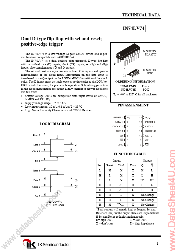
PIN ASSIGNMENT
RESET 1
1 2 3 4 5 6 7
14 13 12 11 10 9 8
V CC RESET 2 DATA2 CLOCK 2 SET 2 Q2 Q2
LOGIC DIAGRAM
DATA 1 CLOCK 1 SET 1 Q1 Q1 GND
FUNCTION TABLE
Inputs Set L H L H H H H H Reset H L L H H H H H L H Clock X X X Data X X X H L X X X Outputs Q H L H* H L Q L H H* L H
w
w
w
.d
e e h s a t a
. u t4
PIN 20=VCC PIN 1...