IPB200N15N3 G IPD200N15N3 G IPI200N15N3 G IPP200N15N3 G
OptiMOS™3 Power-Transistor
Features • N-channel, normal level •...
IPB200N15N3 G IPD200N15N3 G IPI200N15N3 G IPP200N15N3 G
OptiMOS™3 Power-Transistor
Features N-channel, normal level Excellent gate charge x R DS(on) product (FOM) Very low on-resistance R DS(on)
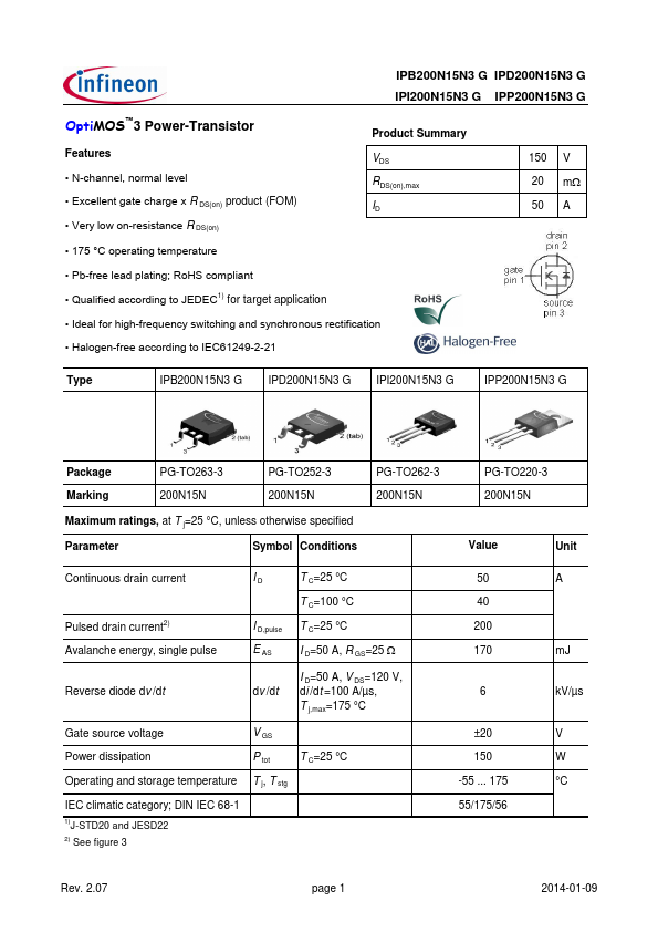
Product Summary VDS RDS(on),max ID
150 V 20 mW 50 A
175 °C operating temperature
Pb-free lead plating; RoHS compliant Qualified according to JEDEC1) for target application
Ideal for high-frequency switching and synchronous rectification
Halogen-free according to IEC61249-2-21
Type
IPB200N15N3 G IPD200N15N3 G IPI200N15N3 G
IPP200N15N3 G
Package
PG-TO263-3
PG-TO252-3
Marking
200N15N
200N15N
Maximum ratings, at T j=25 °C, unless otherwise specified
Parameter
Symbol Conditions
PG-TO262-3 200N15N
PG-TO220-3 200N15N
Value
Unit
Continuous drain current
Pulsed drain current2) Avalanche energy, single pulse
ID
I D,pulse E AS
T C=25 °C T C=100 °C T C=25 °C I D=50 A, R GS=25 W
Reverse diode dv /dt
dv /dt
I D=50 A, V DS=120 V, di /dt =100 A/µs, T j,max=175 °C
Gate source
voltage
V GS
Power dissipation
P tot
T C=25 °C
Operating and storage temperature T j, T stg
IEC climatic category; DIN IEC 68-1 1)J-STD20 and JESD22 2) See figure 3
50 40 200 170
6
±20 150 -55 ... 175 55/175/56
A
mJ kV/µs V W °C
Rev. 2.07
page 1
2014-01-09
IPB200N15N3 G IPD200N15N3 G IPI200N15N3 G IPP200N15N3 G
Parameter
Symbol Conditions
min.
Values typ.
Unit max.
Thermal characteristics
Thermal resistance, junction - case R thJC
-
Thermal resistance, junction am...