OptiMOS®-T2 Power-Transistor
• N-channel - Enhancement mode • Automotive AEC Q101 qualified • MSL1 up to 260°C peak refl...
OptiMOS®-T2 Power-Transistor
N-channel - Enhancement mode Automotive AEC Q101 qualified MSL1 up to 260°C peak reflow 175°C operating temperature Green product (RoHS compliant) 100% Avalanche tested
IPD50N03S4L-06
Product Summary V DS R DS(on),max ID
30 V 5.5 mW 50 A
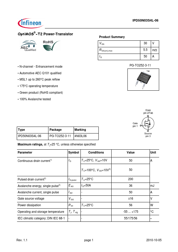
PG-TO252-3-11
Type IPD50N03S4L-06
Package
Marking
PG-TO252-3-11 4N03L06
Maximum ratings, at T j=25 °C, unless otherwise specified
Parameter
Symbol
Conditions
Continuous drain current1)
I D T C=25°C, V GS=10V
T C=100°C, V GS=10V2)
Pulsed drain current2)
I D,pulse T C=25°C
Avalanche energy, single pulse2) E AS I D=50A
Avalanche current, single pulse
I AS -
Gate source
voltage
V GS
-
Power dissipation
P tot T C=25°C
Operating and storage temperature T j, T stg -
IEC climatic category; DIN IEC 68-1 -
-
Value 50
50
200 36 50 ±16 56 -55 ... +175 55/175/56
Unit A
mJ A V W °C -
Rev. 1.1
page 1
2010-10-05
Parameter
IPD50N03S4L-06
Symbol
Conditions
min.
Values typ.
Unit max.
Thermal resistance, junction - case SMD version, device on PCB
R thJC R thJA
minimal footprint 6 cm2 cooling area3)
-
- 2.7 K/W - 62 - 40
Electrical characteristics, at T j=25 °C, unless otherwise specified
Static characteristics Drain-source breakdown
voltage Gate threshold
voltage Zero gate
voltage drain current
Gate-source leakage current Drain-source on-state resistance
V (BR)DSS V GS=0V, I D= 1mA V GS(th) V DS=V GS, I D=20µA
I DSS
V DS=30V, V GS=0V, T j=25°C
V DS=30V, V GS=0V, T j=125°C...