www.DataSheet4U.com
IPB08CN10N G IPI08CN10N G IPP08CN10N G
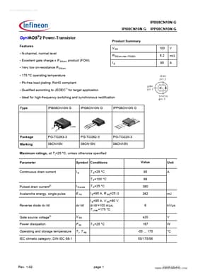
OptiMOS®2 Power-Transistor
Features • N-channel, normal lev...
www.DataSheet4U.com
IPB08CN10N G IPI08CN10N G IPP08CN10N G
OptiMOS®2 Power-Transistor
Features N-channel, normal level Excellent gate charge x R DS(on) product (FOM) Very low on-resistance R DS(on) 175 °C operating temperature Pb-free lead plating; RoHS compliant Qualified according to JEDEC1) for target application
Product Summary V DS R DS(on),max (TO263) ID 100 8.2 95 V mΩ A
Ideal for high-frequency switching and synchronous rectification Type IPB08CN10N G IPI08CN10N G IPP08CN10N G
Package Marking
PG-TO263-3 08CN10N
PG-TO262-3 08CN10N
PG-TO220-3 08CN10N
Maximum ratings, at T j=25 °C, unless otherwise specified Parameter Continuous drain current Symbol Conditions ID T C=25 °C T C=100 °C Pulsed drain current2) Avalanche energy, single pulse Reverse diode dv /dt Gate source
voltage3) Power dissipation Operating and storage temperature IEC climatic category; DIN IEC 68-1 I D,pulse E AS dv /dt V GS P tot T j, T stg T C=25 °C T C=25 °C I D=95 A, R GS=25 Ω I D=95 A, V DS=80 V, di /dt =100 A/µs, T j,max=175 °C Value 95 68 380 262 6 ±20 167 -55 ... 175 55/175/56 mJ kV/µs V W °C Unit A
Rev. 1.02
page 1
2006-06-02
www.DataSheet4U.com
IPB08CN10N G IPI08CN10N G
Parameter Symbol Conditions min. Thermal characteristics Thermal resistance, junction - case Thermal resistance, junction 4) ambient (TO220, TO262, TO263) R thJC R thJA minimal footprint 6 cm2 cooling area5) 0.9 62 40 K/W
IPP08CN10N G
Unit max.
Values typ.
Electrical characteristics, at T j=25 °C, ...