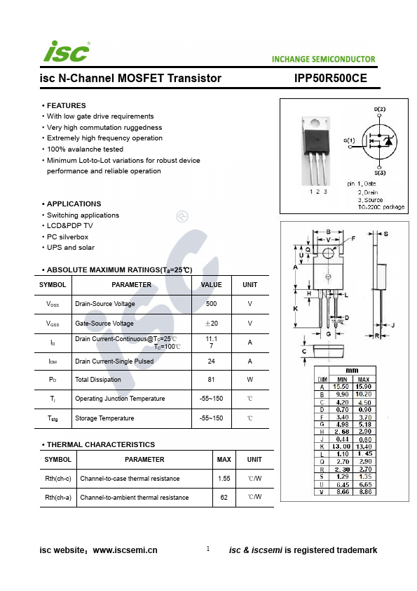
isc N-Channel MOSFET Transistor
·FEATURES ·With low gate drive requirements ·Very high commutation ruggedness ·Extremely...
isc N-Channel
MOSFET Transistor
·FEATURES ·With low gate drive requirements ·Very high commutation ruggedness ·Extremely high frequency operation ·100% avalanche tested ·Minimum Lot-to-Lot variations for robust device
performance and reliable operation
INCHANGE Semiconductor
IPP50R500CE
·APPLICATIONS ·Switching applications ·LCD&PDP TV ·PC silverbox ·UPS and solar
·ABSOLUTE MAXIMUM RATINGS(Ta=25℃)
SYMBOL
PARAMETER
VALUE
VDSS
Drain-Source
Voltage
500
VGSS ID IDM PD
Gate-Source
Voltage Drain Current-Continuous@TC=25℃
TC=100℃ Drain Current-Single Pulsed
Total Dissipation
±20 11.1
7 24
81
Tj
Operating Junction Temperature
-55~150
Tstg
Storage Temperature
-55~150
UNIT V V A A W ℃ ℃
·THERMAL CHARACTERISTICS
SYMBOL
PARAMETER
Rth(ch-c) Channel-to-case thermal resistance
Rth(ch-a) Channel-to-ambient thermal resistance
MAX 1.55 62
UNIT ℃/W ℃/W
isc website:www.iscsemi.cn
1 isc & iscsemi is registered trademark
isc N-Channel
MOSFET Transistor
INCHANGE Semiconductor
IPP50R500CE
ELECTRICAL CHARACTERISTICS
TC=25℃ unless otherwise specified
SYMBOL
PARAMETER
CONDITIONS
MIN TYP MAX UNIT
BVDSS
Drain-Source Breakdown
Voltage VGS=0V; ID= 0.25mA
VGS(th)
Gate Threshold
Voltage
VDS=±20V; ID=1.4mA
RDS(on)
Drain-Source On-Resistance
VGS= 10V; ID=2.3A
IGSS
Gate-Source Leakage Current
VGS= ±20V;VDS= 0V
IDSS
Drain-Source Leakage Current
VDS= 500V; VGS= 0V
VSDF
Diode forward
voltage
ISD=2.9A, VGS = 0 V
500
V
2.5
3.5
V
450 500
mΩ
±0.1 μA
1
μA
0...