IPD05N03LA IPU05N03LA
OptiMOS®2 Power-Transistor
Features • Ideal for high-frequency dc/dc converters • Qualified accor...
IPD05N03LA IPU05N03LA
OptiMOS®2 Power-Transistor
Features Ideal for high-frequency dc/dc converters Qualified according to JEDEC for target application N-channel Logic level Excellent gate charge x R DS(on) product (FOM) Very low on-resistance R DS(on) Superior thermal resistance 175 °C operating temperature dv /dt rated
1)
Product Summary V DS R DS(on),max (SMD version) ID 25 5.1 50 V mΩ A
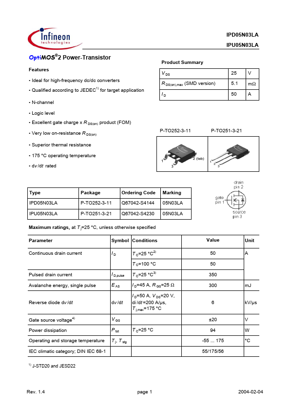
P-TO252-3-11
P-TO251-3-21
Type IPD05N03LA IPU05N03LA
Package P-TO252-3-11 P-TO251-3-21
Ordering Code Q67042-S4144 Q67042-S4230
Marking 05N03LA 05N03LA
Maximum ratings, at T j=25 °C, unless otherwise specified Parameter Continuous drain current Symbol Conditions ID T C=25 °C2) T C=100 °C Pulsed drain current Avalanche energy, single pulse Reverse diode dv /dt Gate source
voltage4) Power dissipation Operating and storage temperature IEC climatic category; DIN IEC 68-1
1)
Value 50 50 350 300 6 ±20
Unit A
I D,pulse E AS dv /dt V GS P tot T j, T stg
T C=25 °C3) I D=45 A, R GS=25 Ω I D=50 A, V DS=20 V, di /dt =200 A/µs, T j,max=175 °C
mJ kV/µs V W °C
T C=25 °C
94 -55 ... 175 55/175/56
J-STD20 and JESD22
Rev. 1.4
page 1
2004-02-04
IPD05N03LA IPU05N03LA
Parameter Symbol Conditions min. Thermal characteristics Thermal resistance, junction - case SMD version, device on PCB R thJC R thJA minimal footprint 6 cm2 cooling area5) Electrical characteristics, at T j=25 °C, unless otherwise specified Static characteristics Drain-source breakdown
voltage Gate threshold ...