www.DataSheet4U.com
IQTCXO-250, -251, -252
ISSUE 7; 14 OCTOBER 2004 Delivery Options
I
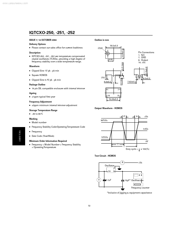
Outline in mm
18.5±0.3 12.0±0.3...
www.DataSheet4U.com
IQTCXO-250, -251, -252
ISSUE 7; 14 OCTOBER 2004 Delivery Options
I
Outline in mm
18.5±0.3 12.0±0.3 Pin Connections 1. N/C 7. GND 8. Output 14. +Vs 1.0±0.2 4.0±0.2 7.62±0.3 tf tr +Vs 1/2Vs 0V t T Duty cycle = t x 100(%) T +Vs 15pF* Oscilloscope Frequency counter *Inclusive of jigging & equipment capacitance
Please contact our sales office for current leadtimes
∅3.8
Description
I
Waveform
I
Clipped Sine 1V pk - pk min Square H
CMOS Clipped Sine 0.7V pk - pk min
4.0±0.2 ∅0.5
I
I
Package Outline
I
14 pin DIL compatible enclosure with internal trimmer
1 14
7 8
Ageing
I
±1ppm typical first year
15.24±0.3
Frequency Adjustment
I
±3ppm minimum internal trimmer adjustment Output Waveform - H
CMOS
Storage Temperature Range
I
–40 to 85°C
90%Vs
Marking
I
Model number Frequency Stability Code/Operating Temperature Code Frequency Date Code (Year/Week)
10%Vs
I
LEADED TCXOs
I
I
Minimum Order Information Required
I
Frequency + Model Number + Frequency Stability + Operating Temperature
Test Circuit - H
CMOS
A Oscillator 7 14 8
V
0.1 µF
72
4.0 min
5.0 max
IQTCXO-250, -251, -252 are temperature compensated crystal oscillators (TCXOs), providing a high degree of frequency stability over a wide temperature range.
6.55
Electrical Specifications - maximum limiting values when measured in test circuit Frequency Range 3.20 to 40.0MHz 3.20 to 40.0MHz 3.20 to 40.0MHz Supply
Voltage 5V±0.25V 5V±0.25V 3V±0.15V Supply Current Output Waveform 5mA 20mA 3mA...