● Trench Technology ● Ultra Low On-Resistance ● P-Channel MOSFET ● Available in Tape & Reel ● Lead-Free
VDSS
-40V
PD -...
● Trench Technology ● Ultra Low On-Resistance ● P-Channel
MOSFET ● Available in Tape & Reel ● Lead-Free
VDSS
-40V
PD - 95294
IRF7241PbF
HEXFET® Power
MOSFET
RDS(on) max (mW)
41@VGS = -10V
70@VGS = -4.5V
ID
-6.2A
-5.0A
Description
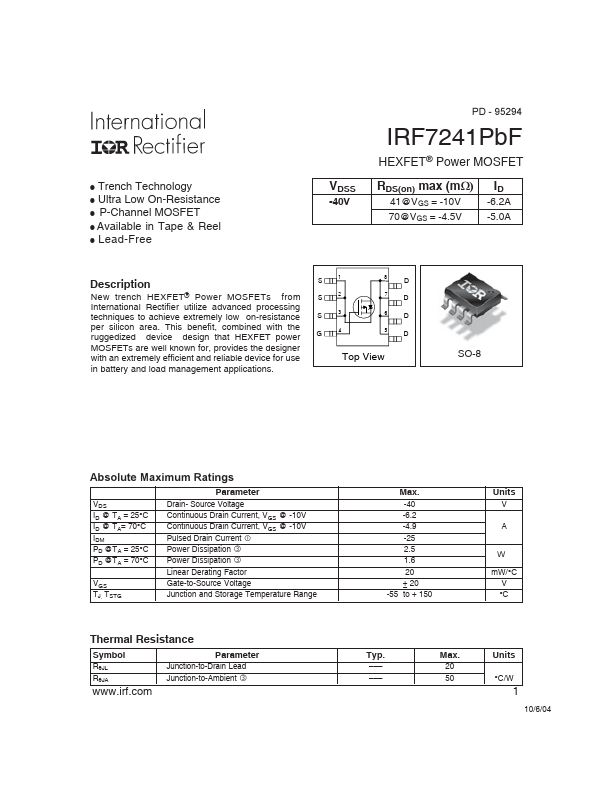
S1
8
A D
New trench HEXFET® Power
MOSFETs from S 2 International Rectifier utilize advanced processing techniques to achieve extremely low on-resistance S 3
7D 6D
per silicon area. This benefit, combined with the ruggedized device design that HEXFET power
G
4
5D
MOSFETs are well known for, provides the designer with an extremely efficient and reliable device for use
Top View
in battery and load management applications.
SO-8
Absolute Maximum Ratings
Parameter
VDS
ID @ TA = 25°C ID @ TA= 70°C IDM PD @TA = 25°C PD @TA = 70°C
Drain- Source
Voltage
Continuous Drain Current, VGS @ -10V Continuous Drain Current, VGS @ -10V Pulsed Drain Current
Power Dissipation Power Dissipation Linear Derating Factor
VGS TJ, TSTG
Gate-to-Source
Voltage Junction and Storage Temperature Range
Thermal Resistance
Symbol
RθJL RθJA
www.irf.com
Parameter Junction-to-Drain Lead Junction-to-Ambient
Max. -40 -6.2 -4.9 -25 2.5 1.6 20 ± 20 -55 to + 150
Units V
A
W mW/°C
V °C
Typ. ––– –––
Max. 20 50
Units
°C/W
1
10/6/04
IRF7241PbF
Electrical Characteristics @ TJ = 25°C (unless otherwise specified)
V(BR)DSS ∆V(BR)DSS/∆TJ
Parameter Drain-to-Source Breakdown
Voltage Breakdown
Voltage Temp. Coefficient
RDS(on)
Static Drain-to-Source On-Resista...