INTEGRATED CIRCUITS DIVISION
Features
• Separate 9A peak source and sink outputs • Operating Voltage Range: -10V to +25V...
INTEGRATED CIRCUITS DIVISION
Features
Separate 9A peak source and sink outputs Operating
Voltage Range: -10V to +25V Internal charge pump regulator for selectable
negative gate drive bias Desaturation detection with soft shutdown sink driver TTL and
CMOS compatible input Under
Voltage lockout (UVLO) Thermal shutdown Open drain FAULT output
Applications
Driving SiC
MOSFETs and IGBTs On-board charger and DC charging station Industrial inverters PFC, AC/DC and DC/DC converters
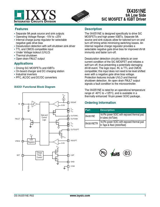
IX4351 Functional Block Diagram
IN 6 FAULT 5
Gate and Control Logic
VREG 8
VDD
4.6V Regulator
SET 9
Charge Pump Control
VDD
6.8V
4 DESAT
2 VDD 3 VDD
1 OUTSRC 16 OUTSNK
15 VSS 10 VSS
14 OUTSOFT
V SS 13 INSOFT
2.6V VDD
12 CAP
11 GND 7 COM
IX4351NE
9A Low Side SiC
MOSFET & IGBT Driver
Description
The IX4351NE is designed specifically to drive SiC
MOSFETs and high power IGBTs. Separate 9A source and sink outputs allow for tailored turn-on and turn-off timing while minimizing switching losses. An internal negative charge regulator provides a selectable negative gate drive bias for improved dV/dt immunity and faster turn-off.
Desaturation detection circuitry detects an over current condition of the SiC
MOSFET and initiates a soft turn off, thus preventing a potentially damaging dV/dt event. The logic input, IN, is TTL and
CMOS compatible; this input does not need to be level shifted even with a negative gate drive bias
voltage. Protection features include UVLO and thermal...