isc P-Channel MOSFET Transistor
·FEATURES ·Static drain-source on-resistance:
RDS(on)≤50mΩ ·100% avalanche tested ·Mini...
isc P-Channel
MOSFET Transistor
·FEATURES ·Static drain-source on-resistance:
RDS(on)≤50mΩ ·100% avalanche tested ·Minimum Lot-to-Lot variations for robust device
performance and reliable operation
·APPLICATION ·Hight side switching ·Current regulators ·Automatic test equipment
·ABSOLUTE MAXIMUM RATINGS(Ta=25℃)
SYMBOL
PARAMETER
VALUE
UNIT
VDSS
Drain-Source
Voltage
-100
V
VGS
Gate-Source
Voltage
±20
V
ID
Drain Current-Continuous
-52
A
IDM
Drain Current-Single Pulsed
-130
A
PD
Total Dissipation @TC=25℃
300
W
Tj
Operating Junction Temperature
-55~150
℃
Tstg
Storage Temperature
-55~150
℃
·THERMAL CHARACTERISTICS
SYMBOL
PARAMETER
Rth(j-c)
Channel-to-case thermal resistance
MAX 0.42
UNIT ℃/W
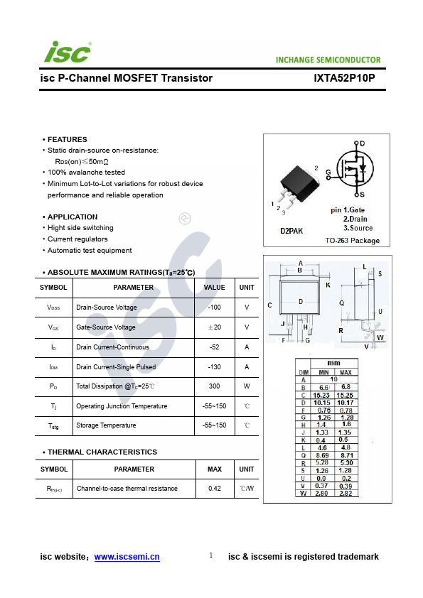
IXTA52P10P
isc website:www.iscsemi.cn
1 isc & iscsemi is registered trademark
isc P-Channel
MOSFET Transistor
IXTA52P10P
ELECTRICAL CHARACTERISTICS
TC=25℃ unless otherwise specified
SYMBOL
PARAMETER
CONDITIONS
MIN TYP MAX UNIT
BVDSS
Drain-Source Breakdown
Voltage VGS=0V; ID= -250μA
-100
V
VGS(th)
Gate Threshold
Voltage
VDS=VGS; ID= -250μA
-2.5
-4.5
V
RDS(on) Drain-Source On-Resistance
VGS= -10V; ID= -26A
50
mΩ
IGSS
Gate-Source Leakage Current
VGS= ±20V
±100 nA
VDS= VDSS; VGS= 0V
IDSS
Drain-Source Leakage Current
VDS= VDSS; VGS= 0V; TJ=125℃
-10 μA
-150
VSD
Diode forward
voltage
IF= -26A; VGS = 0V
-3.5
V
NOTICE: ISC reserves the rights to make changes of the content herein the datasheet at any time without notificati...