IXZR16N60 & IXZR16N60A/B Z-MOS RF Power MOSFET
N-ChaNnCnehlaEnnheal EncnehmanecnetmMeondteMSowdietch Mode RF MOSFET
Low...
IXZR16N60 & IXZR16N60A/B Z-MOS RF Power
MOSFET
N-ChaNnCnehlaEnnheal EncnehmanecnetmMeondteMSowdietch Mode RF
MOSFET
Low CLaopwacQitgaanncde RZg-MOSTM
MOSFET Process OptimHiziegdh fdovr/RdtF Operation
Ideal fNoranColassescoCn,dDS, w&itEchAinpgplications
VDSS ID25
= 600 V = 18 A
Symbol VDSS VDGR
Test Conditions
TJ = 25°C to 150°C TJ = 25°C to 150°C; RGS = 1 MΩ
Maximum Ratings
600
V
600
V
RDS(on) ≤ 0.56 Ω
PDC
=
350
VGS VGSM
Continuous Transient
±20
V
±30
V
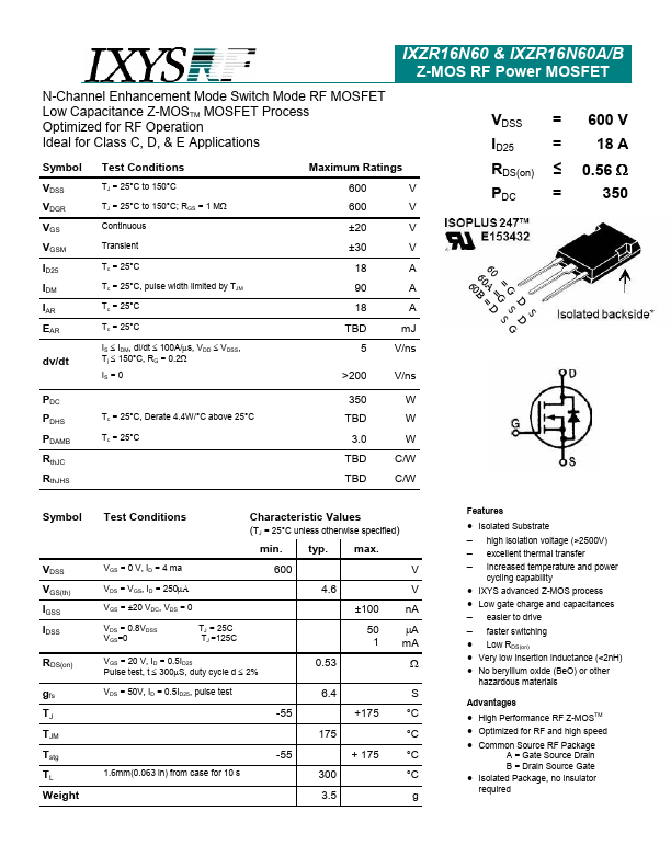
60
S
DD
GS
= =G 60A60B =
ID25
Tc = 25°C
IDM
Tc = 25°C, pulse width limited by TJM
18
A
90
A
D
IAR EAR
Tc = 25°C Tc = 25°C
18
A
TBD
mJ
G S
dv/dt
IS ≤ IDM, di/dt ≤ 100A/µs, VDD ≤ VDSS, Tj ≤ 150°C, RG = 0.2Ω
IS = 0
5 >200
V/ns V/ns
PDC PDHS PDAMB RthJC RthJHS
Tc = 25°C, Derate 4.4W/°C above 25°C Tc = 25°C
350
W
TBD
W
3.0
W
TBD C/W
TBD C/W
Symbol
VDSS VGS(th) IGSS IDSS
RDS(on)
gfs TJ TJM Tstg TL Weight
Test Conditions
Characteristic Values (TJ = 25°C unless otherwise specified)
min. typ. max.
VGS = 0 V, ID = 4 ma
600
V
VDS = VGS, ID = 250µΑ
4.6
V
VGS = ±20 VDC, VDS = 0
±100 nA
VDS = 0.8VDSS VGS=0
TJ = 25C TJ =125C
50 µA 1 mA
VGS = 20 V, ID = 0.5ID25
0.53
Ω
Pulse test, t ≤ 300µS, duty cycle d ≤ 2%
VDS = 50V, ID = 0.5ID25, pulse test
6.4
S
-55
+175 °C
175
°C
-55
+ 175 °C
1.6mm(0.063 in) from case for 10 s
300
°C
3.5
g
Features
Isolated Substrate − high isolation
voltage (>2500V) − excellent thermal transfer − Increased temperature and power
cyc...