www.DataSheet4U.com
J110 JFET − General Purpose
N−Channel − Depletion
N−Channel Junction Field Effect Transistors, depl...
www.DataSheet4U.com
J110 JFET − General Purpose
N−Channel − Depletion
N−Channel Junction Field Effect Transistors, depletion mode (Type A) designed for general purpose audio
amplifiers, analog switches and choppers.
Features
http://onsemi.com
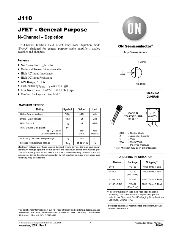
1 DRAIN
N−Channel for Higher Gain Drain and Source Interchangeable High AC Input Impedance High DC Input Resistance Low RDS(on) < 18 W Fast Switching td(on) + tr = 8.0 ns (Typ) Low Noise en = 6.0 nV/√Hz @ 10 Hz (Typ) Pb−Free Packages are Available*
3 GATE
2 SOURCE
MARKING DIAGRAM
MAXIMUM RATINGS
Rating Gate−Source
Voltage Drain −Gate
Voltage Gate Current Total Device Dissipation @ TA = 25°C Derate above 25°C Operating Junction Temp Range Storage Temperature Range Symbol VGS VDG IG PD 310 2.82 TJ Tstg 135 −65 to +150 mW mW/°C °C °C J110 = Device Code A = Assembly Location Y = Year WW = Work Week G = Pb−Free Package (Note: Microdot may be in either location) Value −25 −25 10 Unit Vdc Vdc mAdc
1 2 3
CASE 29 TO−92 (TO−226) STYLE 5
J110 AYWW G G
Maximum ratings are those values beyond which device damage can occur. Maximum ratings applied to the device are individual stress limit values (not normal operating conditions) and are not valid simultaneously. If these limits are exceeded, device functional operation is not implied, damage may occur and reliability may be affected.
ORDERING INFORMATION
Device J110 J110G J110RLRA J110RLRAG Package TO−92 TO−92 (Pb−Free) TO−92 TO−92 (Pb−Free) Shipping † 1000 Units / Box 1000...