J111 / J112 / J113 / MMBFJ111 / MMBFJ112 / MMBFJ113 — N-Channel Switch
January 2015
J111 / J112 / J113 / MMBFJ111 / MM...
J111 / J112 / J113 / MMBFJ111 / MMBFJ112 / MMBFJ113 — N-Channel Switch
January 2015
J111 / J112 / J113 / MMBFJ111 / MMBFJ112 / MMBFJ113 N-Channel Switch
Features
This device is designed for low level analog switching, sample and hold circuits and chopper stabilized
amplifiers.
Sourced from process 51 Source & Drain are interchangeable.
G SD
TO-92
Figure 1. J111 / J112 / J113 Device Package
Ordering Information
Part Number J111
J111_D26Z J111_D74Z
J112 J112_D26Z J112_D27Z J112_D74Z
J113 J113_D74Z J113_D75Z MMBFJ111 MMBFJ112 MMBFJ113
Top Mark J111 J111 J111 J112 J112 J112 J112 J113 J113 J113 6P 6R 6S
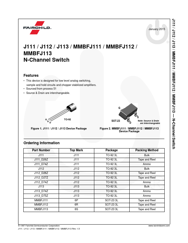
G
SOT-23
S
Note: Source & Drain D are interchangeable
Figure 2. MMBFJ111 / MMBFJ112 / MMBFJ113 Device Package
Package TO-92 3L TO-92 3L TO-92 3L TO-92 3L TO-92 3L TO-92 3L TO-92 3L TO-92 3L TO-92 3L TO-92 3L SOT-23 3L SOT-23 3L SOT-23 3L
Packing Method Bulk
Tape and Reel Ammo Bulk
Tape and Reel Tape and Reel
Ammo Bulk Ammo Ammo Tape and Reel Tape and Reel Tape and Reel
© 1997 Fairchild Semiconductor Corporation J111 / J112 / J113 / MMBFJ111 / MMBFJ112 / MMBFJ113 Rev. 1.5
www.fairchildsemi.com
J111 / J112 / J113 / MMBFJ111 / MMBFJ112 / MMBFJ113 — N-Channel Switch
Absolute Maximum Ratings(1), (2)
Stresses exceeding the absolute maximum ratings may damage the device. The device may not function or be operable above the recommended operating conditions and stressing the parts to these levels is not recommended. In addition, extended exposure to stresses above t...