2SK3017
TOSHIBA Field Effect Transistor Silicon N Channel MOS Type (π−MOSIII)
2SK3017
DC−DC Converter, Relay Drive and ...
2SK3017
TOSHIBA Field Effect Transistor Silicon N Channel MOS Type (π−MOSIII)
2SK3017
DC−DC Converter, Relay Drive and Motor Drive Applications
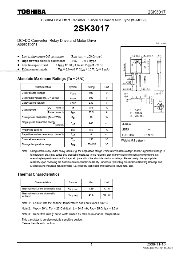
z Low drain−source ON resistance z High forward transfer admittance z Low leakage current z Enhancement mode www.DataSheet4U.com : RDS (ON) = 1.05 Ω (typ.) : |Yfs| = 7.0 S (typ.) Unit: mm
: IDSS = 100 μA (max) (VDS = 720 V) : Vth = 2.0~4.0 V (VDS = 10 V, ID = 1 mA)
Absolute Maximum Ratings (Ta = 25°C)
Characteristics Drain−source
voltage Drain−gate
voltage (RGS = 20 kΩ) Gate−source
voltage Drain current DC (Note 1) Symbol VDSS VDGR VGSS ID IDP PD EAS IAR EAR Tch Tstg Rating 900 900 ±30 8.5 25.5 90 966 8.5 9 150 −55~150 Unit V V V A A W mJ A mJ °C °C
Pulse (Note 1)
Drain power dissipation (Tc = 25°C) Single pulse avalanche energy (Note 2) Avalanche current Repetitive avalanche energy (Note 3) Channel temperature Storage temperature range
JEDEC JEITA TOSHIBA
— — 2-16F1B
Weight: 5.8 g (typ.)
Note: Using continuously under heavy loads (e.g. the application of high temperature/current/
voltage and the significant change in
temperature, etc.) may cause this product to decrease in the reliability significantly even if the operating conditions (i.e. operating temperature/current/
voltage, etc.) are within the absolute maximum ratings. Please design the appropriate reliability upon reviewing the Toshiba Semiconductor Reliability Handbook (“Handling Precautions”/Derating Concept and Methods) and individual reliability data (i.e. reliabil...