www.DataSheet4U.com
SMD Type
N-Channel 60-V (D-S), 175 KI4559EY MOSFET
IC IC
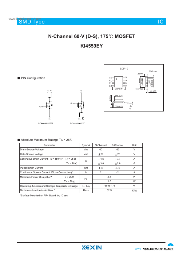
PIN Configuration
Absolute Maximum Rati...
www.DataSheet4U.com
SMD Type
N-Channel 60-V (D-S), 175 KI4559EY
MOSFET
IC IC
PIN Configuration
Absolute Maximum Ratings TA = 25
Parameter Drain-Source
Voltage Gate-Source
Voltage Continuous Drain Current (TJ = 150 )* TA = 25 TA = 70 Pulsed Drain Current Continuous Source Current (Diode Conduction)* Maximum Power Dissipation* TA = 25 TA = 70 Operating Junction and Storage Temperature Range Maximum Junction-to-Ambient * *Surface Mounted on FR4 Board, t 10 sec. TJ, Tstg RthJA IDM IS PD Symbol VDS VGS ID N-Channel 60 20 4.5 3.8 30 2 2.4 1.7 -55 to 175 62.5 /W P-Channel -60 20 3.1 2.6 30 -2 Unit V V A A A A W W
www.kexin.com.cn
1
www.DataSheet4U.com
SMD Type
KI4559EY
Electrical Characteristics TJ = 25
Parameter Gate Threshold
Voltage Gate Body Leakage Symbol VGS( th) IGSS Testconditons VDS = VGS, ID = 250 A VDS = VGS, ID = -250 VDS = 0 V VGS = 20 V VDS = 0 V VGS = 20 V VDS = 60V, VGS = 0 V Zero Gate
Voltage Drain Current IDSS VDS = -60V, VGS = 0 V VDS = 60 V, VGS = 0 V, TJ = 55 VDS = -60V, VGS = 0 V, TJ =55 On State Drain Currenta ID(on) VDS VDS 5 V, VGS = 10 V -5 V, VGS = -10 V A N-Ch P-Ch N-Ch P-Ch N-Ch P-Ch N-Ch P-Ch N-Ch P-Ch N-Ch P-Ch N-Ch P-Ch N-Ch P-Ch N-Ch P-Ch N-Ch P-Ch N-Ch P-Channel VDS = -30 V, VGS = -10 V, ID = -3.1A N Channel VDD = 30 V, RL = 30 ID= 1A, VGEN = 10V, Rg = 6 P-Ch N-Ch P-Ch N-Ch P-Ch N-Ch P-Ch P-Channel VDD = -30 V, RL = 30 Fall Time Source-Drain Reverse Recovery Time * Pulse test; pulse width tf trr ID= -1 A, VGEN = -10 V, Rg = 6 IF = 2 A, di/dt...