SEMICONDUCTOR
TECHNICAL DATA
GENERAL DESCRIPTION
This Trench MOSFET has better characteristics, such as low on resistanc...
SEMICONDUCTOR
TECHNICAL DATA
GENERAL DESCRIPTION
This Trench
MOSFET has better characteristics, such as low on resistance, low gate charge and excellent avalanche characteristiscs. It is mainly suitable for battery protection circuit.
FEATURES VDSS=-40V, ID=-7.5A. Drain-Source ON Resistance. RDS(ON)=30m (Max.) @ VGS=-10V RDS(ON)=37m (Max.) @ VGS=-4.5V Super High Dense Cell Design
MOSFET Maximum Ratings (Ta=25 Unless otherwise noted)
CHARACTERISTIC
SYMBOL PATING UNIT
Drain Source
Voltage
Gate Source
Voltage
Drain Current
DC@Ta=25 Pulsed
Drain Source Diode Forward Current
Drain Power Dissipation DC@Ta=25
Maximum Junction Temperature
Storage Temperature Range
VDSS VGSS ID* IDP
IS PD* Tj Tstg
-40 20
-7.5 -30 -30 2.0 150 -55~150
V V A A A W
Thermal Resistance, Junction to Ambient
RthJA*
62.5
/W
Note : *Surface Mounted on 1” 1” FR4 Board, t 10sec
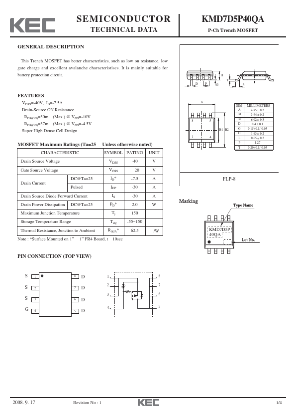
PIN CONNECTION (TOP VIEW)
S1 S2 S3 G4
8D 7D 6D 5D
1 2 3
4
8 7 6
5
KMD7D5P40QA
P-Ch Trench
MOSFET
DP
H T
G
L
A 85
DIM A B1 B2 D
MILLIMETERS 4.85 +_ 0.2 3.94 +_ 0.2 6.02+_ 0.3 0.4 +_ 0.1
B1 B2
G 0.15+0.1/-0.05
H 1.63 +_ 0.2
14
L 0.65 +_ 0.2
P 1.27
T 0.20+0.1/-0.05
FLP-8
KMD7D5P 40QA
2008. 9. 17
Revision No : 1
1/4
KMD7D5P40QA
ELECTRICAL CHARACTERISTICS (Ta=25 ) UNLESS OTHERWISE NOTED
CHARACTERISTIC
SYMBOL
TEST CONDITION
Static
Drain-Source Breakdown
Voltage Drain Cut-off Current Gate Leakage Current Gate Threshold
Voltage
Drain-Source ON Resistance
Forward Transconductance
BVDSS IDSS IGSS V...