SEMICONDUCTOR
TECHNICAL DATA
General Description
This Super Junction MOSFET has better characteristics, such as fast s...
SEMICONDUCTOR
TECHNICAL DATA
General Description
This Super Junction
MOSFET has better characteristics, such as fast switching time, low on resistance, low gate charge and excellent avalanche characteristics. It is mainly suitable for active power factor correction and switching mode power supplies.
FEATURES VDSS=650V, ID=8A Drain-Source ON Resistance : RDS(ON)(Max)=0.62 @VGS=10V Qg(typ.)= 21nC
MAXIMUM RATING (Tc=25 )
CHARACTERISTIC
SYMBOL
RATING
Drain-Source
Voltage Gate-Source
Voltage
VDSS VGSS
650 30
@TC=25
Drain Current @TC=100
Pulsed (Note1)
Single Pulsed Avalanche Energy (Note 2)
Repetitive Avalanche Energy (Note 1)
Peak Diode Recovery dv/dt (Note 3)
Drain Power Dissipation
Tc=25 Derate above 25
ID IDP EAS EAR dv/dt
PD
8 5 18* 50
2.3
4.5 78 0.62
Maximum Junction Temperature Storage Temperature Range Thermal Characteristics
Tj Tstg
150 -55 150
Thermal Resistance, Junction-to-Case RthJC
Thermal Resistance, Junction-to-Ambient
RthJA
* : Drain current limited by maximum junction temperature.
1.6 110
UNIT V V
A
mJ mJ V/ns W W/
/W /W
PIN CONNECTION
D
KP8N65D/I
N CHANNEL MOS FIELD EFFECT TRANSISTOR
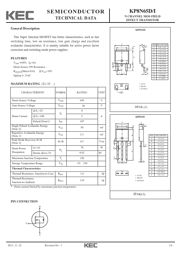
KP8N65D
A CD
B
H G
FF
J E
K L
N M
DIM MILLIMETERS A 6.60 +_ 0.20 B 6.10 +_0.20 C 5.34 +_ 0.30 D 0.70 +_0.20 E 2.70 +_ 0.15 F 2.30 +_ 0.10 G 0.96 MAX
H 0.90 MAX J 1.80 +_0.20 K 2.30 +_0.10 L 0.50 +_ 0.10 M 0.50 +_0.10
N 0.70 MIN
O 0.1 MAX
123
O
1. GATE 2. DRAIN 3. SOURCE
DPAK (1)
KP8N65I
AH CJ
BD
M N
G FF
123
K
E
P
L
1. GATE 2. DRAIN 3. SOURCE...