HERMETIC SILICON PHOTOTRANSISTOR
L14C1
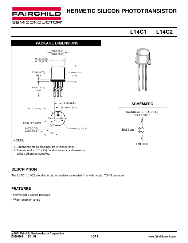
PACKAGE DIMENSIONS
0.230 (5.84) 0.209 (5.31) 0.195 (4.96) 0.178 (4.52)
L14C2
0...
HERMETIC SILICON PHOTOTRANSISTOR
L14C1
PACKAGE DIMENSIONS
0.230 (5.84) 0.209 (5.31) 0.195 (4.96) 0.178 (4.52)
L14C2
0.030 (0.76) MAX
0.210 (5.34) MAX
0.500 (12.7) MIN
0.100 (2.54) 0.100 (2.54) DIA. 2 1 0.038 (.97) NOM 0.046 (1.16) 0.036 (0.92) 45° Ø0.021 (0.53) 3X 3 0.050 (1.27)
SCHEMATIC
(CONNECTED TO CASE) COLLECTOR 3
BASE 2
NOTES: 1. Dimensions for all drawings are in inches (mm). 2. Tolerance of ± .010 (.25) on all non-nominal dimensions unless otherwise specified.
1 EMITTER
DESCRIPTION
The L14C1/L14C2 are silicon phototransistors mounted in a wide angle, TO-18 package.
FEATURES
Hermetically sealed package Wide reception angle
2001 Fairchild Semiconductor Corporation DS300305 6/01/01
1 OF 4
www.fairchildsemi.com
HERMETIC SILICON PHOTOTRANSISTOR
L14C1
ABSOLUTE MAXIMUM RATINGS
Parameter Operating Temperature Storage Temperature Soldering Temperature (Iron)(3,4,5 and 6) Soldering Temperature (Flow)(3,4 and 6) Collector to Emitter Breakdown
Voltage Collector to Base Breakdown
Voltage Emitter to Base Breakdwon
Voltage Power Dissipation (TA = 25°C)(1) Power Dissipation (TC = 25°C)(2) (TA = 25°C unless otherwise specified) Symbol TOPR TSTG TSOL-I TSOL-F VCEO VCBO VEBO PD PD Rating -65 to +125 -65 to +150 240 for 5 sec 260 for 10 sec 50 50 7 300 600
L14C2
Unit °C °C °C °C V V V mW mW
NOTE: 1. Derate power dissipation linearly 3.00 mW/°C above 25°C ambient. 2. Derate power dissipation linearly 6.00 mW/°C above 25°C case. 3. RMA flux is recommended. 4. Meth...