Summary of Specification for OIS & CL-AF Control LSI
LC898129DP1XHTBG
Overview LC898129DP1XHTBG is a system LSI integra...
Summary of Specification for OIS & CL-AF Control LSI
LC898129DP1XHTBG
Overview LC898129DP1XHTBG is a system LSI integrating an on−chip
32 bit DSP, a FLASH ROM and peripherals including analog circuits for OIS (Optical Image Stabilization) / Closed Loop−AF (Auto Focus) control and drivers.
Features
On−chip 32 bit DSP
♦ Built−in Software for Digital Servo Filter ♦ Built−in Software for Gyro Filter
Memory
♦ Flash Memory ♦ Program ROM ♦ Program SRAM ♦ Data SRAM
Peripherals
♦ AD Converter ♦ DA Converter ♦ 2−wire Serial I/F Circuit (The Communication Protocol is
Compatible with I2C) ♦ Hall Bias Circuit ♦ Hall Amp ♦ OSC (Oscillator) ♦ LDO (Low Drop−Out Regulator) ♦ Digital Gyro I/F (SPI) ♦ Interrupt I/F
Driver
♦ OIS Linear Driver (x2ch, Ifull = 200 mA)
♦ CL−AF (bi−direction) Linear Driver (x1ch, Ifull = 150 mA)
Power Supply
Voltage
♦ AD/DA/VGA/LDO/OSC/Flash: AVDD30 = 2.7 V to 3.3 V ♦ Driver: VM = 1.8 V to 3.3 V ♦ 1.8 V I/O: IOVDD = 1.7 V to 3.3 V ♦ Core Logic: Generated by On−chip LDO
Connect 1 mF Capacitor to LDPO pin
Package
♦ WLCSP40 (4 x 10 Pin) Thickness Max. 0.35 mm, with Back Coat
These Devices are Pb−Free, Halogen Free/BFR Free
and are RoHS Compliant
www.onsemi.com
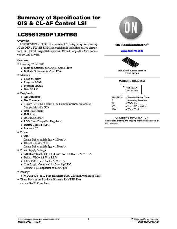
WLCSP40, 1.60x4.15x0.33 CASE 567XS
MARKING DIAGRAM
898129XH AWLYYWW
898129XH A WL YY WW
= Specific Device Code = Assembly Location = Wafer Lot = Year of Production = Work Week
ORDERING INFORMATION
See detailed ordering and shipping information on page 8 of this data sheet.
© Semiconductor Co...