LMH6502 Wideband, Low Power, Linear-in-dB Variable Gain Amplifier
June 2004
LMH6502 Wideband, Low Power, Linear-in-dB ...
LMH6502 Wideband, Low Power, Linear-in-dB Variable Gain Amplifier
June 2004
LMH6502 Wideband, Low Power, Linear-in-dB Variable Gain Amplifier
General Description
The LMH™6502 is a wideband DC coupled differential input
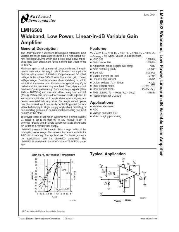
voltage controlled gain stage followed by a high-speed current feedback Op Amp which can directly drive a low impedance load. Gain adjustment range is more than 70dB for up to 10MHz. Maximum gain is set by external components and the gain can be reduced all the way to cut-off. Power consumption is 300mW with a speed of 130MHz. Output referred DC offset
voltage is less than 350mV over the entire gain control
voltage range. Device-to-device Gain matching is within ± 0.6dB at maximum gain. Furthermore, gain at any VG is tested and the tolerance is guaranteed. The output current feedback Op Amp allows high frequency large signals (Slew Rate = 1800V/µs) and can also drive heavy load current (75mA). Differential inputs allow common mode rejection in low level amplification or in applications where signals are carried over relatively long wires. For single ended operation, the unused input can easily be tied to ground (or to a virtual half-supply in single supply application). Inverting or non-inverting gains could be obtained by choosing one input polarity or the other. To provide ease of use when working with a single supply, VG range is set to be from 0V to +2V relative to pin 11 potential (ground pin). In single supply operation, this ground pin is tied to a "vi...