Product Folder
Sample & Buy
Technical Documents
Tools & Software
Support & Community
LMK04803, LMK04805, LMK04806, ...
Product Folder
Sample & Buy
Technical Documents
Tools & Software
Support & Community
LMK04803, LMK04805, LMK04806, LMK04808
SNAS489K – MARCH 2011 – REVISED DECEMBER 2014
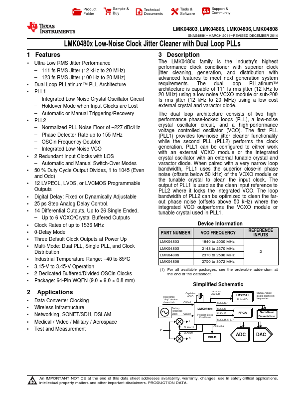
LMK0480x Low-Noise Clock Jitter Cleaner with Dual Loop PLLs
1 Features
1 Ultra-Low RMS Jitter Performance – 111 fs RMS Jitter (12 kHz to 20 MHz) – 123 fs RMS Jitter (100 Hz to 20 MHz)
Dual Loop PLLatinum™ PLL Architecture PLL1
– Integrated Low-Noise Crystal Oscillator Circuit – Holdover Mode when Input Clocks are Lost – Automatic or Manual Triggering/Recovery PLL2 – Normalized PLL Noise Floor of –227 dBc/Hz – Phase Detector Rate up to 155 MHz – OSCin Frequency-Doubler – Integrated Low-Noise VCO 2 Redundant Input Clocks with LOS – Automatic and Manual Switch-Over Modes 50 % Duty Cycle Output Divides, 1 to 1045 (Even and Odd) 12 LVPECL, LVDS, or LV
CMOS Programmable Outputs Digital Delay: Fixed or Dynamically Adjustable 25 ps Step Analog Delay Control. 14 Differential Outputs. Up to 26 Single Ended. – Up to 6 VCXO/Crystal Buffered Outputs Clock Rates of up to 1536 MHz 0-Delay Mode Three Default Clock Outputs at Power Up Multi-Mode: Dual PLL, Single PLL, and Clock Distribution Industrial Temperature Range: –40 to 85°C 3.15-V to 3.45-V Operation 2 Dedicated Buffered/Divided OSCin Clocks Package: 64-Pin WQFN (9.0 × 9.0 × 0.8 mm)
2 Applications
Data Converter Clocking Wireless Infrastructure Networking, SONET/SDH, DSLAM Medical / Video / Military / Aerospace Test an...