Product Folder
Order Now
Technical Documents
Tools & Software
Support & Community
LMK04821, LMK04826, LMK04828
SNAS...
Product Folder
Order Now
Technical Documents
Tools & Software
Support & Community
LMK04821, LMK04826, LMK04828
SNAS605AS – MARCH 2013 – REVISED MAY 2020
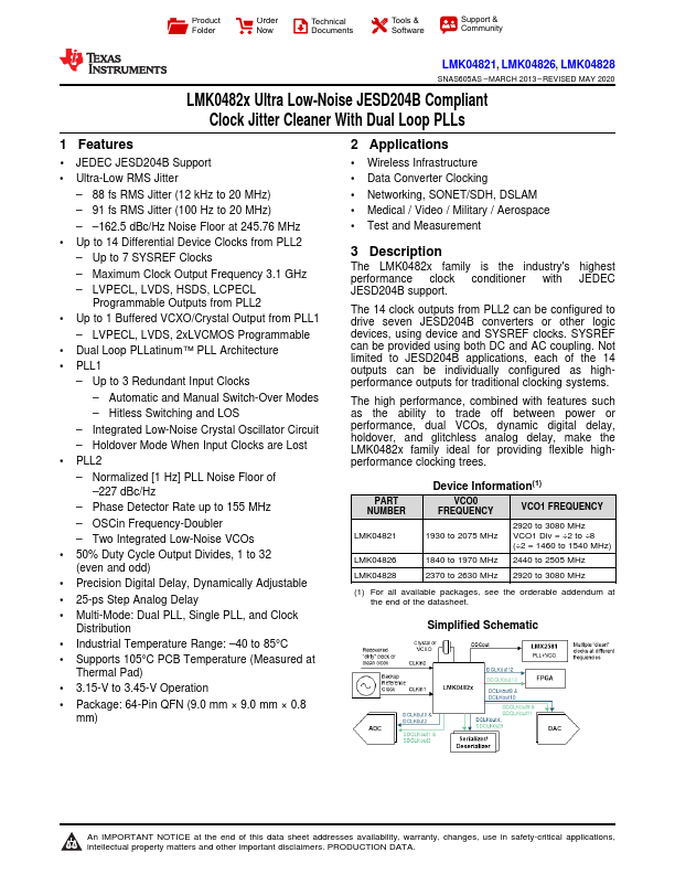
LMK0482x Ultra Low-Noise JESD204B Compliant Clock Jitter Cleaner With Dual Loop PLLs
1 Features
1 JEDEC JESD204B Support Ultra-Low RMS Jitter
– 88 fs RMS Jitter (12 kHz to 20 MHz) – 91 fs RMS Jitter (100 Hz to 20 MHz) – –162.5 dBc/Hz Noise Floor at 245.76 MHz Up to 14 Differential Device Clocks from PLL2 – Up to 7 SYSREF Clocks – Maximum Clock Output Frequency 3.1 GHz – LVPECL, LVDS, HSDS, LCPECL
Programmable Outputs from PLL2 Up to 1 Buffered VCXO/Crystal Output from PLL1
– LVPECL, LVDS, 2xLV
CMOS Programmable Dual Loop PLLatinum™ PLL Architecture PLL1
– Up to 3 Redundant Input Clocks – Automatic and Manual Switch-Over Modes – Hitless Switching and LOS
– Integrated Low-Noise Crystal Oscillator Circuit – Holdover Mode When Input Clocks are Lost PLL2 – Normalized [1 Hz] PLL Noise Floor of
–227 dBc/Hz – Phase Detector Rate up to 155 MHz – OSCin Frequency-Doubler – Two Integrated Low-Noise VCOs 50% Duty Cycle Output Divides, 1 to 32 (even and odd) Precision Digital Delay, Dynamically Adjustable 25-ps Step Analog Delay Multi-Mode: Dual PLL, Single PLL, and Clock Distribution Industrial Temperature Range: –40 to 85°C Supports 105°C PCB Temperature (Measured at Thermal Pad) 3.15-V to 3.45-V Operation Package: 64-Pin QFN (9.0 mm × 9.0 mm × 0.8 mm)
2 Applications
Wireless Infrastructure Data Con...