Product Folder
Sample & Buy
Technical Documents
Tools & Software
Support & Community
Reference Design
LP5912
SNVSA...
Product Folder
Sample & Buy
Technical Documents
Tools & Software
Support & Community
Reference Design
LP5912
SNVSA77D – DECEMBER 2015 – REVISED NOVEMBER 2016
LP5912 500-mA Low-Noise, Low-IQ LDO
1 Features
1 Input
Voltage Range: 1.6 V to 6.5 V Output
Voltage Range: 0.8 V to 5.5 V Output Current up to 500 mA Low Output-
Voltage Noise: 12 µVRMS Typical PSRR at 1 kHz: 75 dB Typical Output
Voltage Tolerance (VOUT ≥ 3.3 V): ±2% Low IQ (Enabled, No Load): 30 µA Typical Low Dropout (VOUT ≥ 3.3 V): 95 mV Typical at
500-mA Load Stable With 1-µF Ceramic Input and Output
Capacitors Thermal-Overload and Short-Circuit Protection Reverse Current Protection No Noise Bypass Capacitor Required Output Automatic Discharge for Fast Turnoff Power-Good Output With 140-µs Typical Delay Internal Soft-Start to Limit the In-rush Current –40°C to +125°C Operating Junction Temperature
Range
2 Applications
Camera Modules Sensors HiFi Audio Radio Transceivers PLL/Synthesizer, Clocking Medium-Current, Noise-Sensitive Applications
space space
3 Description
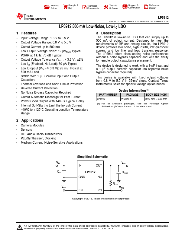
The LP5912 is low-noise LDO that can supply up to 500 mA of output current. Designed to meet the requirements of RF and analog circuits, the LP5912 device provides low noise, high PSRR, low quiescent current, and low line and load transient response. The LP5912 offers class-leading noise performance without a noise bypass capacitor and with the ability for remote output capacitance placement.
The device is de...