www.DataSheet4U.com
RF Power Field Effect Transistor LDMOS, 800—1700 MHz, 15W, 26V
1/11/06
Preliminary
MAPL-000817-0...
www.DataSheet4U.com
RF Power Field Effect Transistor LDMOS, 800—1700 MHz, 15W, 26V
1/11/06
Preliminary
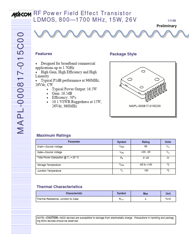
MAPL-000817-015C00
Features
Designed for broadband commercial applications up to 1.7GHz High Gain, High Efficiency and High Linearity Typical P1dB performance at 960MHz, 26Vdc, CW Typical Power Output: 16.5W Gain: 16.5dB Efficiency: 50% 10:1 VSWR Ruggedness at 15W, 26Vdc, 960MHz
Package Style
MAPL-000817-015C00
Maximum Ratings
Parameter Drain—Source
Voltage Gate—Source
Voltage Total Power Dissipation @ TC = 25 °C Storage Temperature Junction Temperature Symbol VDSS VGS PD TSTG TJ Rating 65 +20, -20 31.25 -65 to +150 150 Units Vdc Vdc W °C °C
Thermal Characteristics
Characteristic Thermal Resistance, Junction to Case Symbol RΘJC Max 4 Unit ºC/W
NOTE—CAUTION—MOS devices are susceptible to damage from electrostatic charge. Precautions in handling and packaging MOS devices should be observed.
RF Power LDMOS Transistor, 800-1700 MHz, 15W, 26V
MAPL-000817-015C00
1/11/06
Preliminary
Characteristic DC CHARACTERISTICS @ 25ºC Drain-Source Breakdown
Voltage (VGS = 0 Vdc, ID = 30 µAdc) Gate Threshold
Voltage (Vds = 26 Vdc, Id = 100 mA) Gate Quiescent
Voltage (Vds = 26 Vdc, Id = 100 mA) Drain-Source On-
Voltage (Vgs = 10 Vdc, Id = 1 A) RF FUNCTIONAL TESTS @ 25ºC (In M/A-COM Test Fixture) (1) Common Source Amplifier Gain (VDD = 26 Vdc, IDQ = 100 mA, f = 960 MHz, POUT = 15 W) Drain Efficiency (VDD = 26 Vdc, IDQ = 100 mA, f = 960 MHz, POUT = 15 W) Input Return Los...