www.DataSheet4U.com
RF Power Field Effect Transistor LDMOS, 865 — 960 MHz, 30W, 26V
5/14/04
Preliminary
MAPLST0810-0...
www.DataSheet4U.com
RF Power Field Effect Transistor LDMOS, 865 — 960 MHz, 30W, 26V
5/14/04
Preliminary
MAPLST0810-030CF
Features
Q
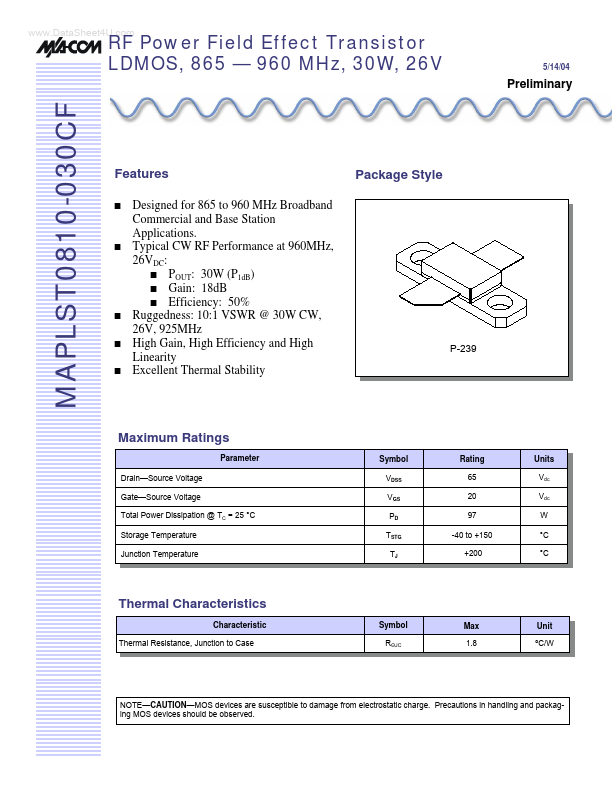
Package Style
Q
Q Q Q
Designed for 865 to 960 MHz Broadband Commercial and Base Station Applications. Typical CW RF Performance at 960MHz, 26VDC: Q POUT: 30W (P1dB) Q Gain: 18dB Q Efficiency: 50% Ruggedness: 10:1 VSWR @ 30W CW, 26V, 925MHz High Gain, High Efficiency and High Linearity Excellent Thermal Stability
P-239
Maximum Ratings
Parameter Drain—Source
Voltage Gate—Source
Voltage Total Power Dissipation @ TC = 25 °C Storage Temperature Junction Temperature Symbol VDSS VGS PD TSTG TJ Rating 65 20 97 -40 to +150 +200 Units Vdc Vdc W °C °C
Thermal Characteristics
Characteristic Thermal Resistance, Junction to Case Symbol RΘJC Max 1.8 Unit ºC/W
NOTE—CAUTION—MOS devices are susceptible to damage from electrostatic charge. Precautions in handling and packaging MOS devices should be observed.
RF Power LDMOS Transistor, 865-960 MHz, 30W, 26V
MAPLST0810-030CF
5/14/04
Preliminary
Characteristic DC CHARACTERISTICS @ 25ºC Drain-Source Breakdown
Voltage (VGS = 0 Vdc, ID = 20 µAdc) Zero Gate
Voltage Drain Leakage Current (VDS = 26 Vdc, VGS = 0) Gate—Source Leakage Current (VGS = 5 Vdc, VDS = 0) Gate Threshold
Voltage (VDS = 10 Vdc, ID = 100 µA) Gate Quiescent
Voltage (VDS = 26 Vdc, ID = 300 mA) Drain-Source On-
Voltage (VGS = 10 Vdc, ID = 1 A) Forward Transconductance (VGS = 10 Vdc, ID = 1 A) DYNAMIC CHARACTERISTICS @ 25ºC Input Capacitance...