www.DataSheet4U.com
RF Power Field Effect Transistor LDMOS, 800—2200 MHz, 2W, 28V
4/14/05
Preliminary
MAPLST0822-002...
www.DataSheet4U.com
RF Power Field Effect Transistor LDMOS, 800—2200 MHz, 2W, 28V
4/14/05
Preliminary
MAPLST0822-002PP
Features
Designed for broadband commercial applications up to 2.2GHz High Gain, High Efficiency and High Linearity Ease of Design for Gain and Insertion Phase Flatness Excellent Thermal Stability W-CDMA Performance at 2.17GHz, 28Vdc Average Output Power: 28dBm @ -39dBc ACPR Gain: 14.5dB (typ.) Efficiency: 23% (typ.) 10:1 VSWR Ruggedness at 2W (CW), 28V, 2.11GHz Performance at 960MHz, 26Vdc, P1dB Average Output Power: 2W min. Gain: 20dB (typ.) Efficiency: 50% (typ.) 10:1 VSWR Ruggedness at 2W, 26V, 960MHz
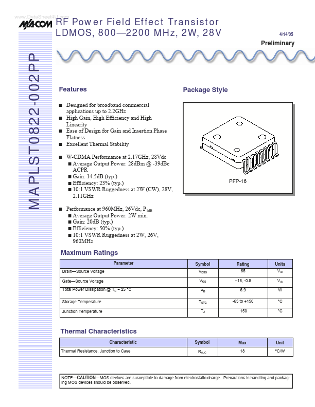
Package Style
PFP-16
Maximum Ratings
Parameter Drain—Source
Voltage Gate—Source
Voltage Total Power Dissipation @ TC = 25 °C Storage Temperature Junction Temperature Symbol VDSS VGS PD TSTG TJ Rating 65 +15, -0.5 6.9 -65 to +150 150 Units Vdc Vdc W °C °C
Thermal Characteristics
Characteristic Thermal Resistance, Junction to Case Symbol RΘJC Max 18 Unit ºC/W
NOTE—CAUTION—MOS devices are susceptible to damage from electrostatic charge. Precautions in handling and packaging MOS devices should be observed.
RF Power LDMOS Transistor, 800-2200 MHz, 2W, 28V
MAPLST0822-002PP
4/14/05
Preliminary
Characteristic DC CHARACTERISTICS @ 25ºC Drain-Source Breakdown
Voltage (VGS = 0 Vdc, ID = 30 µAdc) Gate Threshold
Voltage (Vds = 26 Vdc, Id = 25 mA) Gate Quiescent
Voltage (Vds = 26 Vdc, Id = 25 mA) Drain-Source On-
Voltage (Vgs = 10 Vdc, Id = 0.1 A) V(BR)DSS VGS(...