www.DataSheet4U.com
RF Power Field Effect Transistor LDMOS, 1800 — 2000 MHz, 30W, 26V
5/14/04
Preliminary
MAPLST1820...
www.DataSheet4U.com
RF Power Field Effect Transistor LDMOS, 1800 — 2000 MHz, 30W, 26V
5/14/04
Preliminary
MAPLST1820-030CF
Features
Designed for base station applications in the 1805-1880MHz or 1930-1990MHz Frequency Band. Suitable for GSM, EDGE, TDMA, CDMA, and multi-carrier amplifier applications
Q Q Q Q Q
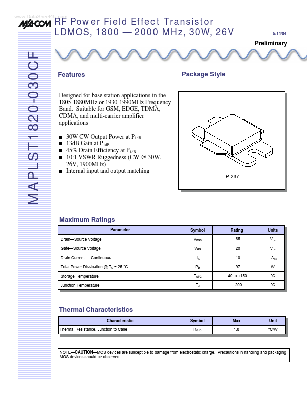
Package Style
30W CW Output Power at P1dB 13dB Gain at P1dB 45% Drain Efficiency at P1dB 10:1 VSWR Ruggedness (CW @ 30W, 26V, 1900MHz) Internal input and output matching
P-237
Maximum Ratings
Parameter Drain—Source
Voltage Gate—Source
Voltage Drain Current — Continuous Total Power Dissipation @ TC = 25 °C Storage Temperature Junction Temperature Symbol VDSS VGS ID PD TSTG TJ Rating 65 20 10 97 -40 to +150 +200 Units Vdc Vdc Adc W °C °C
Thermal Characteristics
Characteristic Thermal Resistance, Junction to Case Symbol RΘJC Max 1.8 Unit ºC/W
NOTE—CAUTION—MOS devices are susceptible to damage from electrostatic charge. Precautions in handling and packaging MOS devices should be observed.
RF Power LDMOS Transistor, 1800 — 2000 MHz, 30W, 26V
MAPLST1820-030CF
5/14/04
Preliminary
Characteristic DC CHARACTERISTICS @ 25ºC Characteristic Drain-Source Breakdown
Voltage GS = 0 Vdc, ID = 20 µAdc) OFF(V CHARACTERISTICS Zero Gate
Voltage Drain Leakage Current 26 Vdc, VGS (VDS DS = 65 GS = 0) Gate—Source Leakage Zero Gate
Voltage DrainCurrent Leakage Current (VGS = = 26 5 Vdc, V 0) DS == (V Vdc, V 0) DS GS Gate Threshold
Voltage Gate—Source Leakage Current (VDS = 10 Vdc, ID...