8-Stage Shift/Store Register
DATA SHEET www.onsemi.com
8-Stage Shift/Store Register with Three-State Outputs
MC14094B
The MC14094B combines an 8−sta...
Description
DATA SHEET www.onsemi.com
8-Stage Shift/Store Register with Three-State Outputs
MC14094B
The MC14094B combines an 8−stage shift register with a data latch for each stage and a 3−state output from each latch.
Data is shifted on the positive clock transition and is shifted from the seventh stage to two serial outputs. The QS output data is for use in high−speed cascaded systems. The QS output data is shifted on the following negative clock transition for use in low−speed cascaded systems.
Data from each stage of the shift register is latched on the negative transition of the strobe input. Data propagates through the latch while strobe is high.
Outputs of the eight data latches are controlled by 3−state buffers which are placed in the high−impedance state by a logic Low on Output Enable.
Features
3−State Outputs Capable of Driving Two Low−Power TTL Loads or One Low−Power
Schottky TTL Load Over the Rated Temperature Range
Input Diode Protection Data Latch Dual Outputs for Data Out on Both Positive and
Negative Clock Transitions
Useful for Serial−to−Parallel Data Conversion Pin−for−Pin Compatible with CD4094B NLV Prefix for Automotive and Other Applications Requiring
Unique Site and Control Change Requirements; AEC−Q100 Qualified and PPAP Capable
These Devices are Pb−Free and are RoHS Compliant
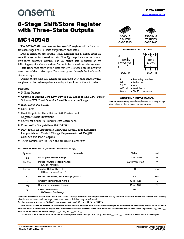
SOIC−16 D SUFFIX CASE 751B
TSSOP−16 DT SUFFIX CASE 948F
MARKING DIAGRAMS
16 14094BG AWLYWW
1
SOIC−16
16 14
094B ALYWG
G
1
TSSOP−16
A WL, L YY, Y WW, W G or G
= Ass...
Similar Datasheet