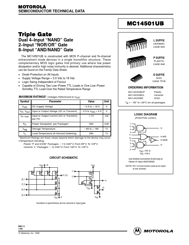
MOTOROLA
SEMICONDUCTOR TECHNICAL DATA
Triple Gate
Dual 4–Input “NAND” Gate
2–Input “NOR/OR” Gate
8–Input “AND/NAND” Gat...
MOTOROLA
SEMICONDUCTOR TECHNICAL DATA
Triple Gate
Dual 4–Input “NAND” Gate
2–Input “NOR/OR” Gate
8–Input “AND/NAND” Gate
The MC14501UB is constructed with MOS P–channel and N–channel enhancement mode devices in a single monolithic structure. These complementary MOS logic gates find primary use where low power dissipation and/or high noise immunity is desired. Additional characteristics can be found on the Family Data Sheet.
Diode Protection on All Inputs
Supply
Voltage Range = 3.0 Vdc to 18 Vdc
Logic Swing Independent of Fanout
Capable of Driving Two Low–Power TTL Loads or One Low–Power
ÎÎÎÎÎÎÎÎÎÎÎÎÎÎÎÎÎÎÎÎÎSchottky TTL Load Over the Rated Temperature Range
ÎÎÎÎÎÎÎÎÎÎÎÎÎÎÎÎÎÎÎÎÎMAXIMUM RATINGS* (
Voltages Referenced to VSS)
ÎÎÎÎÎÎÎÎÎÎÎÎÎÎÎÎÎÎÎÎÎSymbol
Parameter
Value
Unit
ÎÎÎÎÎÎÎÎÎÎÎÎÎÎÎÎÎÎÎÎÎVDD DC Supply
Voltage ÎÎÎÎÎÎÎÎÎÎÎÎÎÎÎÎÎÎÎÎÎVin, Vout Input or Output
Voltage (DC or Transient) ÎÎÎÎÎÎÎÎÎÎÎÎÎÎÎÎÎÎÎÎÎIin, Iout Input or Output Current (DC or Transient), ÎÎÎÎÎÎÎÎÎÎÎÎÎÎÎÎÎÎÎÎÎper Pin
– 0.5 to + 18.0 – 0.5 to VDD + 0.5
± 10
V V mA
ÎÎÎÎÎÎÎÎÎÎÎÎÎÎÎÎÎÎÎÎÎPD Power Dissipation, per Package† ÎÎÎÎÎÎÎÎÎÎÎÎÎÎÎÎÎÎÎÎÎTstg Storage Temperature ÎÎÎÎÎÎÎÎÎÎÎÎÎÎÎÎÎÎÎÎÎÎÎÎÎÎÎÎÎÎÎÎÎÎÎÎÎÎÎÎÎÎTL Lead Temperature(8–SecondSoldering)
500 – 65 to + 150
260
mW _C _C
* Maximum Ratings are those values beyond which damage to the device may occur.
†Temperature Derating:
Plastic “P and D/DW” Packages: – 7.0 mW/_C From 65_C To 125_C
Ceramic “L” Packages: – 12 mW/_C From 100_C ...