MOTOROLA
SEMICONDUCTOR TECHNICAL DATA
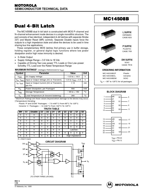
Dual 4-Bit Latch
The MC14508B dual 4–bit latch is constructed with MOS P–channel...
MOTOROLA
SEMICONDUCTOR TECHNICAL DATA
Dual 4-Bit Latch
The MC14508B dual 4–bit latch is constructed with MOS P–channel and N–channel enhancement mode devices in a single monolithic structure. The part consists of two identical, independent 4–bit latches with separate Strobe (ST) and Master Reset (MR) controls. Separate Disable inputs force the outputs to a high impedance state and allow the devices to be used in time sharing bus line applications.
These complementary MOS latches find primary use in buffer storage, holding register, or general digital logic functions where low power dissipation and/or high noise immunity is desired.
3–State Output
Supply
Voltage Range = 3.0 Vdc to 18 Vdc
ÎÎÎÎÎÎÎÎÎÎÎÎÎÎÎÎÎÎÎÎÎ Capable–of Driving Two Low–power TTL Loads or One Low–power Schottky TTL Load over the Rated Temperature Range
ÎÎÎÎÎÎÎÎÎÎÎÎÎÎÎÎÎÎÎÎÎÎÎÎÎÎÎÎÎÎÎÎÎÎÎÎÎÎÎÎÎÎMAXIMUM RATINGS* (
Voltages Referenced to VSS)
Symbol
Parameter
Value
Unit
VDD Vin, Vout Iin, Iout
DC Supply
Voltage
Input or Output
Voltage (DC or Transient)
Input or Output Current (DC or Transient), per Pin
– 0.5 to + 18.0
– 0.5 to VDD + 0.5 ± 10
V V mA
PD Power Dissipation, per Package† Tstg Storage Temperature
500 – 65 to + 150
mW _C
TL Lead Temperature (8–Second Soldering)
260 _C
* Maximum Ratings are those values beyond which damage to the device may occur.
†Temperature Derating:
Plastic “P and D/DW” Packages: – 7.0 mW/_C From 65_C To 125_C
Ceramic “L” Packages: – 12 mW/_C From 100_C To 125...