MOTOROLA
SEMICONDUCTOR TECHNICAL DATA
Product Preview
MC54/74HC175A
J SUFFIX CERAMIC PACKAGE CASE 620–10
1
Quad D Fl...
MOTOROLA
SEMICONDUCTOR TECHNICAL DATA
Product Preview
MC54/74HC175A
J SUFFIX CERAMIC PACKAGE CASE 620–10
1
Quad D Flip-Flop with Common Clock and Reset
High–Performance Silicon–Gate
CMOS
The MC54/74HC175A is identical in pinout to the LS175. The device inputs are compatible with standard
CMOS outputs; with pullup resistors, they are compatible with LSTTL outputs. This device consists of four D flip–flops with common Reset and Clock inputs, and separate D inputs. Reset (active–low) is asynchronous and occurs when a low level is applied to the Reset input. Information at a D input is transferred to the corresponding Q output on the next positive going edge of the Clock input. Output Drive Capability: 10 LSTTL Loads Outputs Directly Interface to
CMOS, NMOS, and TTL Operating
Voltage Range: 2 to 6 V Low Input Current: 1 µA High Noise Immunity Characteristic of
CMOS Devices In Compliance with the Requirements Defined by JEDEC Standard No. 7A Chip Complexity 166 FETs or 41.5 Equivalent Gates
16
16 1
N SUFFIX PLASTIC PACKAGE CASE 648–08
16 1
D SUFFIX SOIC PACKAGE CASE 751B–05
16 1
DT SUFFIX TSSOP PACKAGE CASE 948F–01
ORDERING INFORMATION
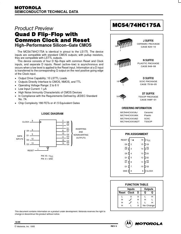
LOGIC DIAGRAM
CLOCK 9 2 3 7 6 10 11 15 14 1 PIN 16 = VCC PIN 8 = GND Q0 Q0 Q1 Q1 Q2 Q2 Q3 Q3
MC54HCXXXAJ MC74HCXXXAN MC74HCXXXAD MC74HCXXXADT INVERTING AND NONINVERTING OUTPUTS
Ceramic Plastic SOIC TSSOP
D0 DATA INPUTS D1
4 5
PIN ASSIGNMENT
RESET Q0 Q0 D0 D1 Q1 Q1 GND 1 2 3 4 5 6 7 8 16 15 14 13 12 11 10 9 VCC Q3 Q3 D3...