MC54/74F174 HEX D FLIP-FLOP WITH MASTER RESET
The MC54/74F174 is a high-speed hex D flip-flop. The device is used primar...
MC54/74F174 HEX D FLIP-FLOP WITH MASTER RESET
The MC54/74F174 is a high-speed hex D flip-flop. The device is used primarily as a 6-bit edge-triggered storage register. The device has a Master Reset to simultaneously clear all flip-flops. The F174 consists of six edge-triggered D flip-flops with individual D inputs and Q outputs. The Clock (CP) and Master Reset (MR) are common to all flip-flops. The state of each D input, one setup time before low-to-high clock transition, is transferred to the corresponding flig-flop’s Q output. A LOW input to the Master Reset (MR) will force all outputs LOW independent of Clock or Data inputs. The F174 is useful for applications where only the true output is required and the Clock and Master Reset are common to all storage elements. Six Edge-triggered D-type Inputs Buffered Positive Edge-triggered Common Clock Buffered, Asynchronous Common Reset
16 1
HEX D FLIP-FLOP WITH MASTER RESET
FAST™ SCHOTTKY TTL
J SUFFIX CERAMIC CASE 620-09
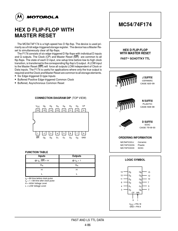
CONNECTION DIAGRAM DIP (TOP VIEW)
VCC 16 Q5 15 D5 14 D4 13 Q4 12 D3 11 Q3 10 CP 9 N SUFFIX PLASTIC CASE 648-08
1
16
16 1
D SUFFIX SOIC CASE 751B-03
1 MR
2 Q0
3 D0
4 D1
5 Q1
6 D2
7 Q2
8 GND
ORDERING INFORMATION
MC54FXXXJ MC74FXXXN MC74FXXXD Ceramic Plastic SOIC
FUNCTION TABLE
Inputs @ tn, MR = H Dn H L
tn = Bit time before clock pulse tn + 1 = Bit time after clock pulse H = HIGH
Voltage Level L = LOW
Voltage Level
Outputs @ tn + 1 Qn H 14 L 13 11 6 4 3 D5 D4 D3 D2 D1 D0 Q5 Q4 Q3 Q2 Q1 Q0 CP MR...