4-BIT PARALLEL ACCESS SHIFT REGISTER
MC74F195 4-BIT PARALLEL ACCESS SHIFT REGISTER
The functional characteristics of the MC74F195 4-Bit Parallel Access Shift...
Description
MC74F195 4-BIT PARALLEL ACCESS SHIFT REGISTER
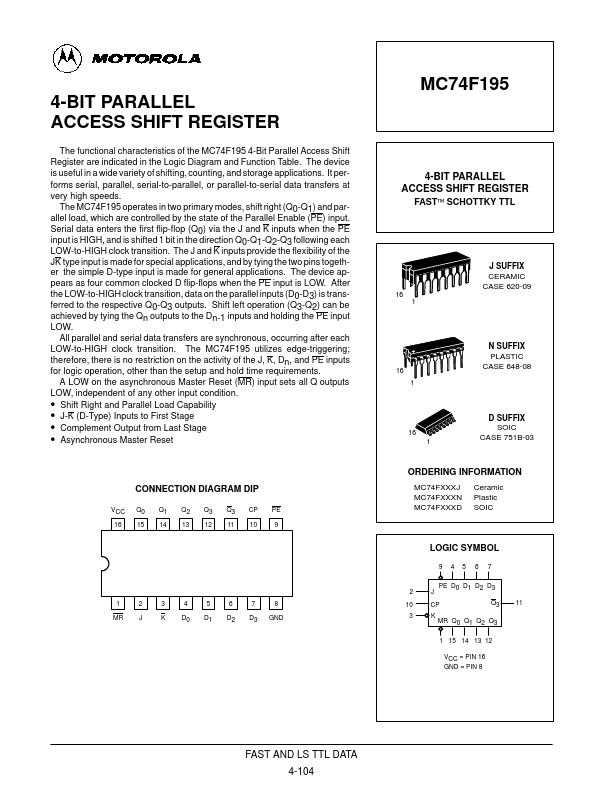
The functional characteristics of the MC74F195 4-Bit Parallel Access Shift Register are indicated in the Logic Diagram and Function Table. The device is useful in a wide variety of shifting, counting, and storage applications. It performs serial, parallel, serial-to-parallel, or parallel-to-serial data transfers at very high speeds. The MC74F195 operates in two primary modes, shift right (Q0-Q1) and parallel load, which are controlled by the state of the Parallel Enable (PE) input. Serial data enters the first flip-flop (Q0) via the J and K inputs when the PE input is HIGH, and is shifted 1 bit in the direction Q0-Q1-Q2-Q3 following each LOW-to-HIGH clock transition. The J and K inputs provide the flexibility of the JK type input is made for special applications, and by tying the two pins together the simple D-type input is made for general applications. The device appears as four common clocked D flip-flops when the PE input is LOW. After the LOW-to-HIGH clock transition, data on the parallel inputs (D0-D3) is transferred to the respective Q0-Q3 outputs. Shift left operation (Q3-Q2) can be achieved by tying the Qn outputs to the Dn-1 inputs and holding the PE input LOW. All parallel and serial data transfers are synchronous, occurring after each LOW-to-HIGH clock transition. The MC74F195 utilizes edge-triggering; therefore, there is no restriction on the activity of the J, K, Dn, and PE inputs for logic operation, other than the ...
Similar Datasheet