MOTOROLA
SEMICONDUCTOR TECHNICAL DATA
Order this document from Logic Marketing
Clock Driver Quad DĆType FlipĆFlop
MC...
MOTOROLA
SEMICONDUCTOR TECHNICAL DATA
Order this document from Logic Marketing
Clock Driver Quad DĆType FlipĆFlop
MC74F803
CLOCK DRIVER QUAD D-TYPE FLIP-FLOP WITH MATCHED PROPAGATION DELAYS
With Matched Propagation Delays
The MC74F803 is a high-speed, low-power, quad D-type flip-flop featuring separate D-type inputs, and inverting outputs with closely matched propagation delays. With a buffered clock (CP) input that is common to all flip-flops, the F803 is useful in high-frequency systems as a clock driver, providing multiple outputs that are synchronous. Because of the matched propagation delays, the duty cycles of the output waveforms in a clock driver application are symmetrical within 1.0 to 1.5 nanoseconds.
Edge-Triggered D-Type Inputs Buffered Positive Edge-Triggered Clock Matched Outputs for Synchronous Clock Driver Applications Outputs Guaranteed for Simultaneous Switching
14 1
J SUFFIX CERAMIC CASE 632-08
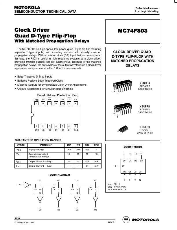
Pinout: 14-Lead Plastic (Top View)
VCC 14 NC 13 O3 12 D3 11 D2 10 O2 9 CP 8
14 1
N SUFFIX PLASTIC CASE 646-06
1 GND
2 NC
3 O0
4 D0
5 D1
6 O1
7 GND
14 1
D SUFFIX SOIC CASE 751A-03
GUARANTEED OPERATION RANGES
Symbol VCC TA IOH IOL Parameter Supply
Voltage Operating Ambient Temperature Range Output Current — High Output Current — Low Min 4.5 0 — — Typ 5.0 25 — — Max 5.5 70 –20 24 Unit V °C mA mA 8
LOGIC SYMBOL
4 D0 CP O0 O1 O2 O3 5 D1 10 D2 11 D3
LOGIC DIAGRAM
D0 CP CP D Q CP D Q CP D Q CP D Q D1 D2 D3 3 VCC = PIN 14 GND = PINS 1 AND 7 NC ...