8MB Synchronous Fast Static RAM Module
MOTOROLA
SEMICONDUCTOR TECHNICAL DATA
Order this document by MCM72F10/D
8MB Synchronous Fast Static RAM Module
The MC...
Description
MOTOROLA
SEMICONDUCTOR TECHNICAL DATA
Order this document by MCM72F10/D
8MB Synchronous Fast Static RAM Module
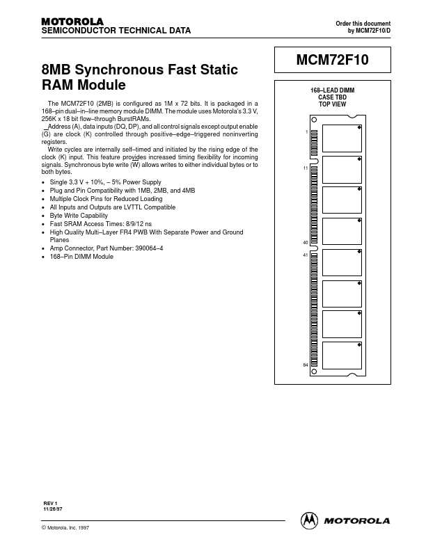
The MCM72F10 (2MB) is configured as 1M x 72 bits. It is packaged in a 168–pin dual–in–line memory module DIMM. The module uses Motorola’s 3.3 V, 256K x 18 bit flow–through BurstRAMs. Address (A), data inputs (DQ, DP), and all control signals except output enable (G) are clock (K) controlled through positive–edge–triggered noninverting registers. Write cycles are internally self–timed and initiated by the rising edge of the clock (K) input. This feature provides increased timing flexibility for incoming signals. Synchronous byte write (W) allows writes to either individual bytes or to both bytes. Single 3.3 V + 10%, – 5% Power Supply Plug and Pin Compatibility with 1MB, 2MB, and 4MB Multiple Clock Pins for Reduced Loading All Inputs and Outputs are LVTTL Compatible Byte Write Capability Fast SRAM Access Times: 8/9/12 ns High Quality Multi–Layer FR4 PWB With Separate Power and Ground Planes Amp Connector, Part Number: 390064–4 168–Pin DIMM Module
MCM72F10
168–LEAD DIMM CASE TBD TOP VIEW
1
11
40 41
84
REV 1 11/26/97
© Motorola, Inc. 1997 MOTOROLA FAST SRAM
MCM72F10 1
BLOCK DIAGRAM
256K x 18
SE1 G A0 – A17 ADSC SBa SBb K DQa0 – DQa7 DQa8 DQb0 – DQb7 DQb8 SE2 ADV ADSP SGW SW LBO SE3
256K x 18
SE1 G A0 – A17 ADSC SBa SBb K DQa0 – DQa7 DQa8 DQb0 – DQb7 DQb8 SE2 ADV ADSP SGW SW LBO SE3
256K x 18
SE1 G A0 – A17 ADSC SBa SBb K DQa0 – DQa7 DQa8 D...
Similar Datasheet