www.DataSheet4U.com
30V N-Channel Enhancement Mode MOSFET
V DS =30V R DS(ON) ,Vgs@10V,Ids@45A=6 m Ù R DS(ON) ,[email protected],...
www.DataSheet4U.com
30V N-Channel Enhancement Mode
MOSFET
V DS =30V R DS(ON) ,Vgs@10V,Ids@45A=6 m Ù R DS(ON) ,
[email protected],Ids@30A=10 m Ù
FEATURES
Advanced trench process technology High Density Cell Design For Ultra Low On-Resistance Specially Designed for DC/DC Converters and Motor Drivers Fully Characterized Avalanche
Voltage and Current
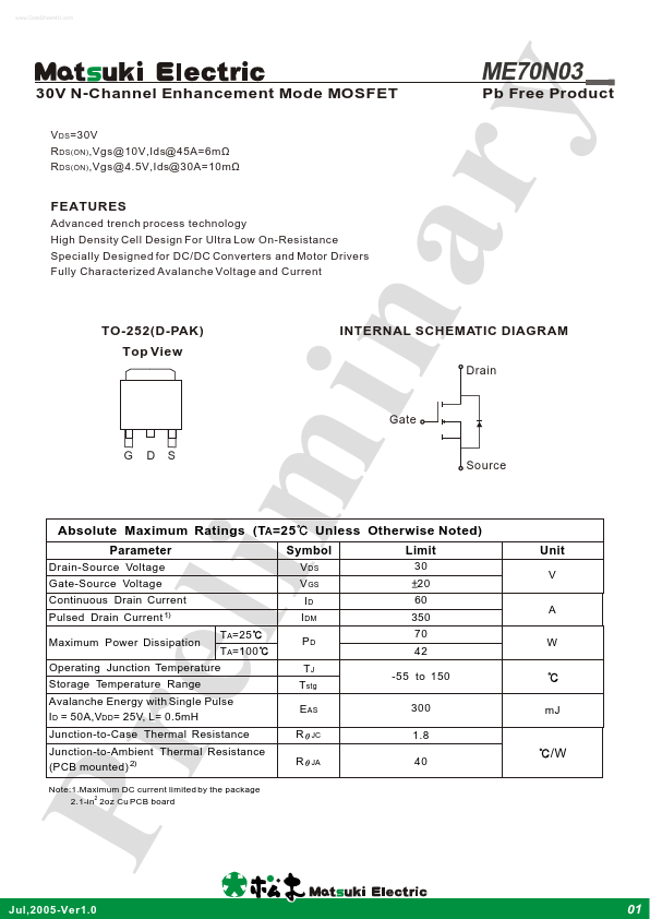
TO-252(D-PAK) Top View
G
D
S
mi
Gate
Absolute Maximum Ratings (TA=25
Parameter
Drain-Source
Voltage Gate-Source
Voltage Pulsed Drain
Symbol
V DS ID V GS I DM PD TJ
na
Drain
INTERNAL SCHEMATIC DIAGRAM
Unless Otherwise Noted)
Limit
30 20 60 350 70 42 -55 to 150 300 1.8 40 mJ
eli
Current 1) T stg E AS R R
JC JA
Continuous Drain Current
T A=25 T A=100 Operating Junction Temperature Storage Temperature Range Maximum Power Dissipation Avalanche Energy with Single Pulse I D = 50A,VDD= 25V, L= 0.5mH
Pr
Jul,2005-Ver1.0
Junction-to-Case Thermal Resistance
Junction-to-Ambient Thermal Resistance (PCB mounted) 2)
Note:1.Maximum DC current limited by the package 2 2.1-in 2oz Cu PCB board
ry
Source
ME70N03
Pb Free Product
Unit
V A W
/W
01
30V N-Channel Enhancement Mode
MOSFET
Electrical Characteristics (T J =25
Symbol
STATIC BVDSS RDS(ON) VGS(th) IDSS IGSS Rg gfs Qg Qgs Qgd Td(on) tr Td(off) tf Ciss Coss Crss Drain-Source Breakdown
Voltage Drain-Source On-State Resistance Gate Threshold
Voltage Zero Gate
Voltage Drain Current Gate-Body Leakage Gate Resistance Forward Transconductance Total Gate Charge Gate-Source Charge Gate-Drain ...