CYStech Electronics Corp.
N-Channel Logic Level Enhancement Mode Power MOSFET
www.DataSheet4U.com Spec. No. : C430J3 Is...
CYStech Electronics Corp.
N-Channel Logic Level Enhancement Mode Power
MOSFET
www.DataSheet4U.com Spec. No. : C430J3 Issued Date : 2008.10.20 Revised Date :2009.02.04 Page No. : 1/7
MEN09N03BJ3
Features
VDS=30V, ID=50A, RDS(ON)=9mΩ Low Gate Charge Simple Drive Requirement RoHS compliant package Repetitive Avalanche Rated Fast Switching Characteristic
BVDSS 30V ID 50A RDSON 9mΩ
Symbol
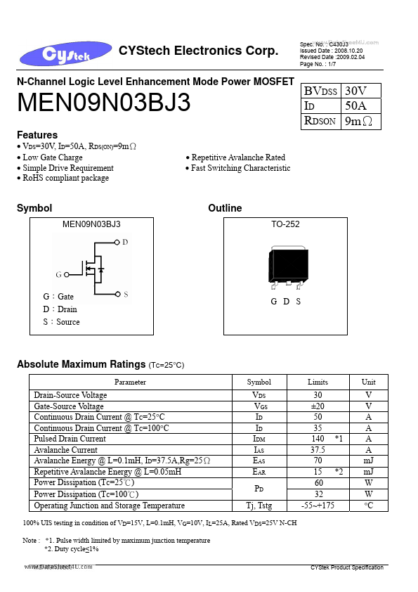
MEN09N03BJ3
Outline
TO-252
G:Gate D:Drain S:Source
G D S
Absolute Maximum Ratings (TC=25°C)
Parameter Symbol Limits Unit
Drain-Source
Voltage Gate-Source
Voltage Continuous Drain Current @ TC=25°C Continuous Drain Current @ TC=100°C Pulsed Drain Current Avalanche Current Avalanche Energy @ L=0.1mH, ID=37.5A,Rg=25Ω Repetitive Avalanche Energy @ L=0.05mH Power Dissipation (TC=25℃) Power Dissipation (TC=100℃) Operating Junction and Storage Temperature
VDS VGS ID ID IDM IAS EAS EAR PD Tj, Tstg
30 ±20 50 35 140 *1 37.5 70 15 *2 60 32 -55~+175
V V A A A A mJ mJ W W °C
100% UIS testing in condition of VD=15V, L=0.1mH, VG=10V, IL=25A, Rated VDS=25V N-CH Note : *1. Pulse width limited by maximum junction temperature *2. Duty cycle≤1%
MEN09N03BJ3 CYStek Product Specification
CYStech Electronics Corp.
Thermal Data
Parameter Thermal Resistance, Junction-to-case, max Thermal Resistance, Junction-to-ambient, max Symbol Rth,j-c Rth,j-a
www.DataSheet4U.com Spec. No. : C430J3 Issued Date : 2008.10.20 Revised Date :2009.02.04 Page No. : 2/7
Value 2.5 75
Unit °C/W °C/W
Characteristics ...