SIDE LOOK PACKAGE NPN PHOTODETECTOR
Description
The MID-11422 is a NPN silicon phototransistor mounted in a lensed ,wate...
SIDE LOOK PACKAGE NPN PHOTODETECTOR
Description
The MID-11422 is a NPN silicon phototransistor mounted in a lensed ,water clear plastic and side looking package.
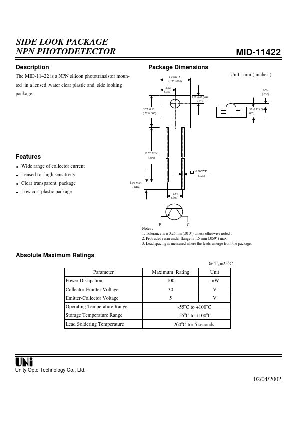
5.72±0.12 (.225±.005)
MID-11422
Package Dimensions
4.45±0.12 (.175±.005) 2.22 (.087)
1.22±0.07 (.048 ±.003)
Unit : mm ( inches )
0.76 (.030)
1.55±0.12 (.061 ±.005)
Features
l l l l
12.70 MIN. (.500)
Wide range of collector current Lensed for high sensitivity Clear transparent package Low cost plastic package
1.00 MIN. (.040) 2.54 (.100) 0.50 TYP. (.020)
E C Notes : 1. Tolerance is ± 0.25mm (.010") unless otherwise noted . 2. Protruded resin under flange is 1.5 mm (.059") max 3. Lead spacing is measured where the leads emerge from the package.
Absolute Maximum Ratings
@ TA=25 C Parameter Power Dissipation Collector-Emitter
Voltage Emitter-Collector
Voltage Operating Temperature Range Storage Temperature Range Lead Soldering Temperature Maximum Rating 100 30 5 -55 C to +100 C -55oC to +100oC 260 C for 5 seconds
o o o o
Unit mW V V
Unity Opto Technology Co., Ltd.
02/04/2002
MID-11422
Optical-Electrical Characteristics
@ TA=25oC Parameter Collector-Emitter Breakdown
Voltage Emitter-Collector Breakdown
Voltage Collector-Emitter Saturation
Voltage Rise Time Fall Time Collector Dark Current On State Collector Current
Iceo-Collector Dark Current-µA
Test Conditions Ie=0.1mA Ee=0 Ie=0.1mA Ee=0 Ic=0.5 mA Ee=0.1mW/cm2 VR =30V , 0=1KΩ IC=1mA VCE=10V Ee=0mW/cm2 VCE=5V Ee=0.1mW/cm2
Symbol V(BR)CEO V(BR)ECO VCE(SAT) Tr...