MJD112 MJD117
Complementary power Darlington transistors
Features
■ Good hFE linearity ■ High fT frequency ■ Monolithic...
MJD112 MJD117
Complementary power Darlington transistors
Features
■ Good hFE linearity ■ High fT frequency ■ Monolithic Darlington configuration with
integrated antiparallel collector-emitter diode
Application
■ Linear and switching industrial equipment
Description
The devices are manufactured in planar technology with “base island” layout and monolithic Darlington configuration.
.
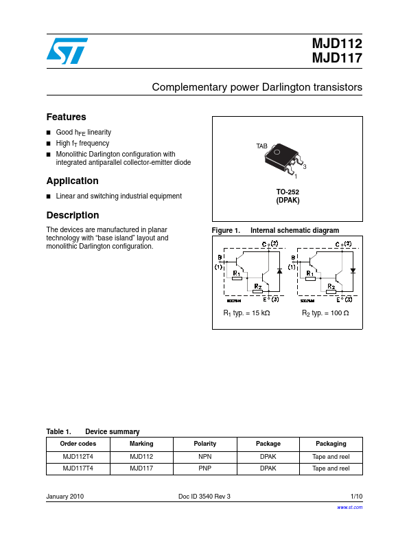
TAB 3
1
TO-252 (DPAK)
Figure 1. Internal schematic diagram
R1 typ. = 15 kΩ
R2 typ. = 100 Ω
Table 1. Device summary
Order codes
Marking
MJD112T4 MJD117T4
MJD112 MJD117
January 2010
Polarity NPN PNP
Doc ID 3540 Rev 3
Package DPAK DPAK
Packaging Tape and reel Tape and reel
1/10
www.st.com
10
Absolute maximum ratings
1
Absolute maximum ratings
Note:
Table 2. Absolute maximum ratings
Symbol
Parameter
VCBO VCEO VEBO
IC ICM IB PTOT TSTG TJ
Collector-base
voltage (IE = 0) Collector-emitter
voltage (IB = 0) Emitter-base
voltage (IC = 0) Collector current Collector peak current Base current Total dissipation at Tcase = 25 °C Storage temperature Max. operating junction temperature
For PNP types
voltage and current values are negative.
Table 3. Thermal data
Symbol
Parameter
RthJC Thermal resistance junction-case max.
MJD112, MJD117
Value
Unit
100
V
5
V
2
A
4
A
0.05
A
20
W
-65 to 150
°C
150
°C
Value 6.25
Unit °C/W
2/10
Doc ID 3540 Rev 3
MJD112, MJD117
2
Electrical characteristics
Electrical characteristics
Note:
Tcase = 25 °C; unless otherwise specified...