CLOCK VCXO PLL
3.3 VOLT COMMUNICATIONS CLOCK VCXO PLL
DATASHEET
MK2049-34
Description
The MK2049-34 is a VCXO Phased Locked Loop (PLL...
Description
3.3 VOLT COMMUNICATIONS CLOCK VCXO PLL
DATASHEET
MK2049-34
Description
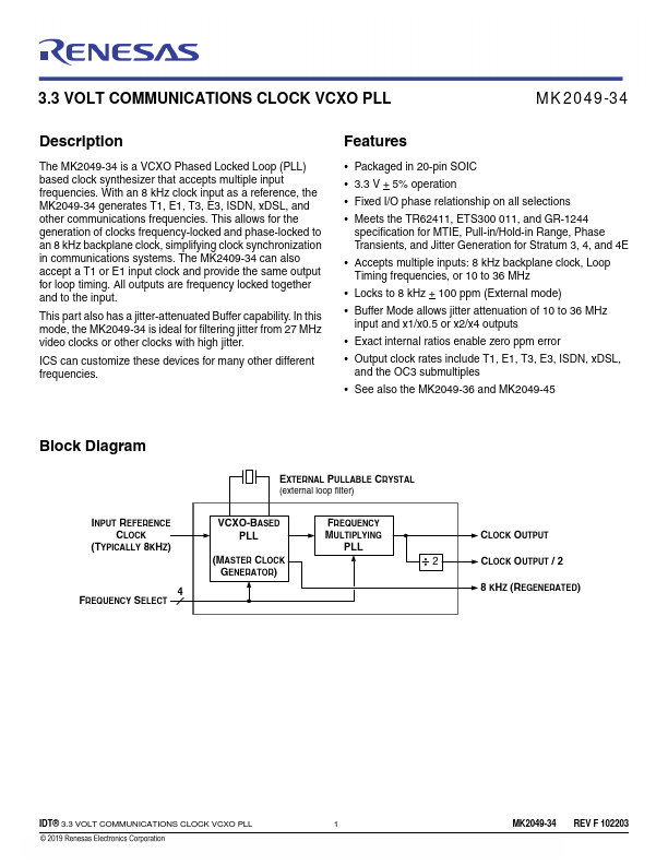
The MK2049-34 is a VCXO Phased Locked Loop (PLL) based clock synthesizer that accepts multiple input frequencies. With an 8 kHz clock input as a reference, the MK2049-34 generates T1, E1, T3, E3, ISDN, xDSL, and other communications frequencies. This allows for the generation of clocks frequency-locked and phase-locked to an 8 kHz backplane clock, simplifying clock synchronization in communications systems. The MK2409-34 can also accept a T1 or E1 input clock and provide the same output for loop timing. All outputs are frequency locked together and to the input.
This part also has a jitter-attenuated Buffer capability. In this mode, the MK2049-34 is ideal for filtering jitter from 27 MHz video clocks or other clocks with high jitter.
ICS can customize these devices for many other different frequencies.
Features
Packaged in 20-pin SOIC 3.3 V + 5% operation Fixed I/O phase relationship on all selections Meets the TR62411, ETS300 011, and GR-1244
specification for MTIE, Pull-in/Hold-in Range, Phase Transients, and Jitter Generation for Stratum 3, 4, and 4E
Accepts multiple inputs: 8 kHz backplane clock, Loop
Timing frequencies, or 10 to 36 MHz
Locks to 8 kHz + 100 ppm (External mode) Buffer Mode allows jitter attenuation of 10 to 36 MHz
input and x1/x0.5 or x2/x4 outputs
Exact internal ratios enable zero ppm error Output clock rates include T1, E1, T3, E3, ISDN, xDSL,
and the OC3 submulti...
Similar Datasheet