MM54HC133 MM74HC133 13-Input NAND Gate
January 1988
MM54HC133 MM74HC133 13-Input NAND Gate
General Description
This NA...
MM54HC133 MM74HC133 13-Input NAND Gate
January 1988
MM54HC133 MM74HC133 13-Input NAND Gate
General Description
This NAND gate utilizes advanced silicon-gate
CMOS technology to achieve operating speeds similar to LS-TTL gates with the low power consumption of standard
CMOS integrated circuits All gates have buffered outputs All devices have high noise immunity and the ability to drive 10 LS-TTL loads The 54HC 74HC logic family is functionally as well as pin-out compatible with the standard 54LS 74LS logic family All inputs are protected from damage due to static discharge by internal diode clamps to VCC and ground
Features
Y Y Y Y Y
Typical propagation delay 20 ns Wide power supply range 2 – 6V Low quiescent current 20 mA maximum (74HC Series) Low input current 1 mA maximum Fanout of 10 LS-TTL loads
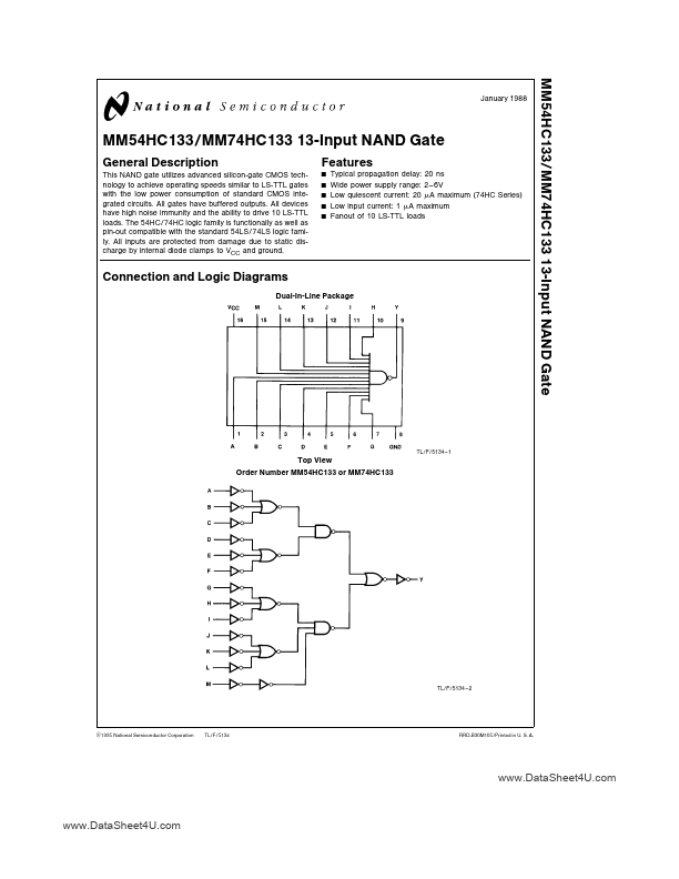
Connection and Logic Diagrams
Dual-In-Line Package
TL F 5134 – 1
Top View Order Number MM54HC133 or MM74HC133
TL F 5134 – 2
C1995 National Semiconductor Corporation
TL F 5134
RRD-B30M105 Printed in U S A
www.DataSheet4U.com
www.DataSheet4U.com
Absolute Maximum Ratings (Notes 1
2)
Operating Conditions
Min Supply
Voltage VCC DC Input or Output
Voltage VIN VOUT Operating Temp Range (TA) MM HC MM HC Input Rise or Fall Times VCC e V tr tf VCC e V VCC e V
b b
If Military Aerospace specified devices are required please contact the National Semiconductor Sales Office Distributors for availability and specifications Supply
Voltage (VCC) DC Input
Voltage (VIN) DC Output Volt...