N-Channel JFET
MMBFJ110
Features
• This Device is Designed for Digital Switching Applications where
Very Low On Resist...
N-Channel JFET
MMBFJ110
Features
This Device is Designed for Digital Switching Applications where
Very Low On Resistance is Mandatory
Sourced from Process 58 This is a Pb−Free Device
MAXIMUM RATINGS (TA = 25°C unless otherwise specified) (Notes 1, 2)
Symbol
Parameter
Value
Unit
VDG Drain−Gate
Voltage
25
V
VGS Gate−Source
Voltage
−25
V
IGF Forward Gate Current
10
mA
TJ
Junction Temperature
150
°C
TJ, TSTG Storage Temperature Range
−55 to 150 °C
Stresses exceeding those listed in the Maximum Ratings table may damage the device. If any of these limits are exceeded, device functionality should not be assumed, damage may occur and reliability may be affected. 1. These ratings are based on a maximum junction temperature of 150°C. 2. These are steady−state limits. ON Semiconductor should be consulted on
applications involving pulsed or low−duty−cycle operations.
THERMAL CHARACTERISTICS (TA = 25°C unless otherwise specified) (Note 3)
Symbol
Parameter
Max Unit
PD Total Device Dissipation Derate Above 25°C
460
mW
3.68 mW/°C
RqJA Thermal Resistance, Junction−to−Ambient
270 °C/W
3. Device mounted on FR−4 PCB 36 mm x 18 mm x 1.5 mm; mounting pad for the collector lead minimum 6 cm2.
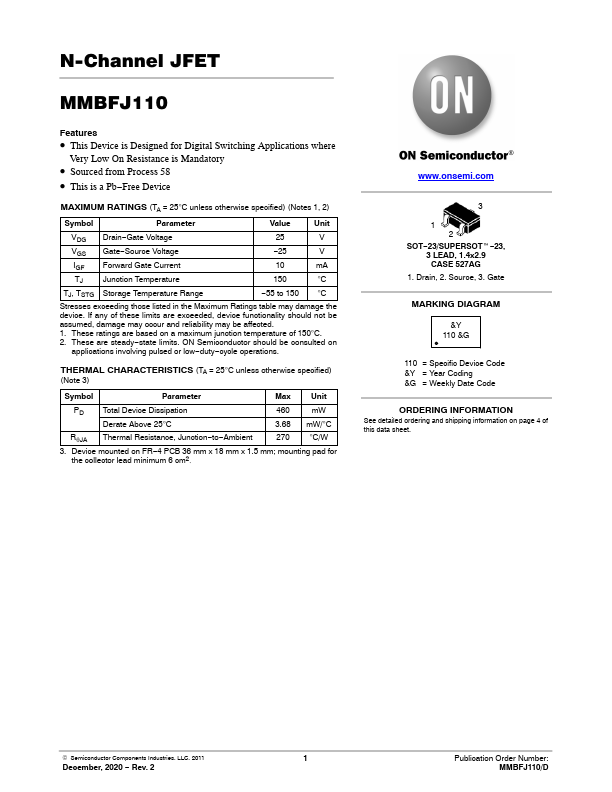
www.onsemi.com
3
1 2
SOT−23/SUPERSOTt−23, 3 LEAD, 1.4x2.9 CASE 527AG
1. Drain, 2. Source, 3. Gate
MARKING DIAGRAM
&Y 110 &G
110 = Specific Device Code &Y = Year Coding &G = Weekly Date Code
ORDERING INFORMATION
See detailed ordering and shipping information on page 4 of...