MOTOROLA
SEMICONDUCTOR TECHNICAL DATA
Order this document by MMBFJ175LT1/D
JFET Chopper
P–Channel — Depletion
2 SOUR...
MOTOROLA
SEMICONDUCTOR TECHNICAL DATA
Order this document by MMBFJ175LT1/D
JFET Chopper
P–Channel — Depletion
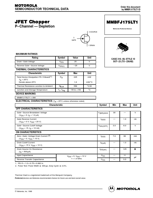
2 SOURCE 3 GATE 1 DRAIN
MMBFJ175LT1
Motorola Preferred Device
3 1
MAXIMUM RATINGS
Rating Drain – Gate
Voltage Reverse Gate – Source
Voltage Symbol VDG VGS(r) Value 25 – 25 Unit V V
2
CASE 318 – 08, STYLE 10 SOT– 23 (TO – 236AB)
THERMAL CHARACTERISTICS
Characteristic Total Device Dissipation FR– 5 Board(1) TA = 25°C Derate above 25°C Thermal Resistance Junction to Ambient Junction and Storage Temperature Symbol PD Max 225 1.8 RqJA TJ, Tstg 556 – 55 to +150 Unit mW mW/°C °C/W °C
DEVICE MARKING
MMBFJ175LT1 = 6W
ELECTRICAL CHARACTERISTICS (TA = 25°C unless otherwise noted)
Characteristic Symbol Min Max Unit
OFF CHARACTERISTICS
Gate – Source Breakdown
Voltage (VDS = 0, ID = 1.0 µA) Gate Reverse Current (VDS = 0 V, VGS = 20 V) Gate – Source Cutoff
Voltage (VDS = 15, ID = 10 nA) V(BR)GSS IGSS VGS(OFF) 30 — 3.0 — 1.0 6.0 V nA V
ON CHARACTERISTICS
Zero – Gate –
Voltage Drain Current (2) (VGS = 0, VDS = 15 V) Drain Cutoff Current (VDS = 15 V, VGS = 10 V) Drain Source On Resistance (ID = 500 mA) Input Capacitance Reverse Transfer Capacitance 1. FR–5 = 1.0 x 0.75 x 0.062 in. 2. Pulse Test: Pulse Width 300 ms, Duty Cycle VDS = 0, VGS = 10 V f = 1.0 MHz IDSS ID(off) rDS(on) Ciss Crss 7.0 — — — — 60 1.0 125 11 pF 5.5 mA nA
W
v
v 2.0%.
Thermal Clad is a registered trademark of the Berquist Company.
Preferred devices are Motorola recommended choices for future use and...