N-Channel RF Amplifier J211, MMBFJ211
Description This device is designed for HF/VHF mixer/amplifier and
applications w...
N-Channel RF Amplifier J211, MMBFJ211
Description This device is designed for HF/VHF mixer/amplifier and
applications where process 50 is not adequate. Sufficient gain and low−noise for sensitive receivers. Sourced from process 90.
MAXIMUM RATINGS (TA = 25°C unless otherwise noted) (Notes 1, 2)
Symbol
Parameter
Value
Unit
VDG VGS IGF TJ, TSTG
Drain−Gate
Voltage
Gate−Source
Voltage
Forward Gate Current
Operating and Storage Junction Temperature Range
25
V
−25
V
10
mA
−55 to 150 °C
Stresses exceeding those listed in the Maximum Ratings table may damage the device. If any of these limits are exceeded, device functionality should not be assumed, damage may occur and reliability may be affected. 1. These ratings are based on a maximum junction temperature of 150°C. 2. These are steady−state limits. onsemi should be consulted on applications
involving pulsed or low− duty−cycle operations.
THERMAL CHARACTERISTICS (TA = 25°C unless otherwise noted) Max
Symbol
Parameter
J211 MMBFJ211 (Note 3) (Note 3) Unit
PD
Total Device Dissipation
Derate Above 25°C
350
225
mW
2.8
1.8
mW/°C
RqJC
Thermal Resistance, Junction−to−Case
125
−
°C/W
RqJA
Thermal Resistance, Junction−to−Ambient
357
556
°C/W
3. Device mounted on FR−4 PCB 36 mm x 18 mm x 1.5 mm; mounting pad for the collector lead minimum 6 cm2.
DATA SHEET www.onsemi.com
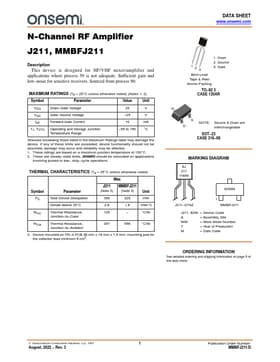
1. Drain
12 3
2. Source 3. Gate
Bent Lead
Tape & Reel
Ammo Packing
TO−92 3 CASE 135AR
G
S
NOTE: Source & Drain are
D
inte...