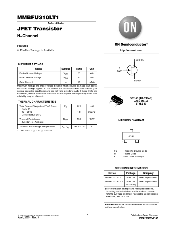
www.DataSheet4U.com
MMBFU310LT1
Preferred Device
JFET Transistor
N−Channel
Features
• Pb−Free Package is Available
h...
www.DataSheet4U.com
MMBFU310LT1
Preferred Device
JFET Transistor
N−Channel
Features
Pb−Free Package is Available
http://onsemi.com
2 SOURCE
MAXIMUM RATINGS
Rating Drain−Source
Voltage Gate−Source
Voltage Gate Current Symbol VDS VGS IG Value 25 25 10 Unit Vdc Vdc mAdc 1 DRAIN 3 GATE
Maximum ratings are those values beyond which device damage can occur. Maximum ratings applied to the device are individual stress limit values (not normal operating conditions) and are not valid simultaneously. If these limits are exceeded, device functional operation is not implied, damage may occur and reliability may be affected.
3 1
THERMAL CHARACTERISTICS
Total Device Dissipation FR− 5 Board (Note 1) TA = 25°C Derate above 25°C Thermal Resistance, Junction−to−Ambient Junction and Storage Temperature 1. FR−5 = 1.0 0.75 0.062 in. PD 225 1.8 RqJA TJ, Tstg 556 −55 to +150 mW mW/°C °C/W °C
SOT−23 (TO−236AB) CASE 318−08 STYLE 10
2
MARKING DIAGRAM
6C M 1
6C M G
= Specific Device Code = Date Code = Pb−Free Package
ORDERING INFORMATION
Device MMBFU310LT1 MMBFU310LT1G Package SOT−23 SOT−23 (Pb−Free) Shipping† 3000 Tape & Reel 3000 Tape & Reel
†For information on tape and reel specifications, including part orientation and tape sizes, please refer to our Tape and Reel Packaging Specifications Brochure, BRD8011/D.
Preferred devices are recommended choices for future use and best overall value.
© Semiconductor Components Industries, LLC, 2005
1
April, 2005 − Rev. 3
Publication ...