MMBT2131T1G
General Purpose Transistors
PNP Bipolar Junction Transistor
NOTE: Voltage and Current are negative for the...
MMBT2131T1G
General Purpose Transistors
PNP Bipolar Junction Transistor
NOTE:
Voltage and Current are negative for the PNP Transistor.
Features
These Devices are Pb−Free and are RoHS Compliant
MAXIMUM RATINGS (TC = 25°C unless otherwise noted)
Rating
Symbol Value
Unit
Collector−Emitter
Voltage Collector−Base
Voltage Emitter−Base
Voltage Collector Current Base Current Total Power Dissipation @ TC = 25°C Total Power Dissipation @ TC = 85°C Thermal Resistance, Junction−to−Ambient (Note 1)
VCEO VCBO VEBO
IC IB PD PD RqJA
30
V
40
V
5.0
V
700
mA
350
mA
342
mW
178
mW
366
°C/W
Total Power Dissipation @ TC = 25°C Total Power Dissipation @ TC = 85°C Thermal Resistance, Junction−to−Ambient (Note 2)
PD PD RqJA
665
mW
346
mW
188
°C/W
Operating and Storage Temperature Range TJ, Tstg −55 to +150 °C
Stresses exceeding Maximum Ratings may damage the device. Maximum Ratings are stress ratings only. Functional operation above the Recommended Operating Conditions is not implied. Extended exposure to stresses above the Recommended Operating Conditions may affect device reliability. 1. Minimum FR−4 or G−10 PCB, Operating to Steady State. 2. Mounted onto a 2″ square FR−4 Board (1″ sq. 2 oz Cu 0.06″ thick single
sided), Operating to Steady State.
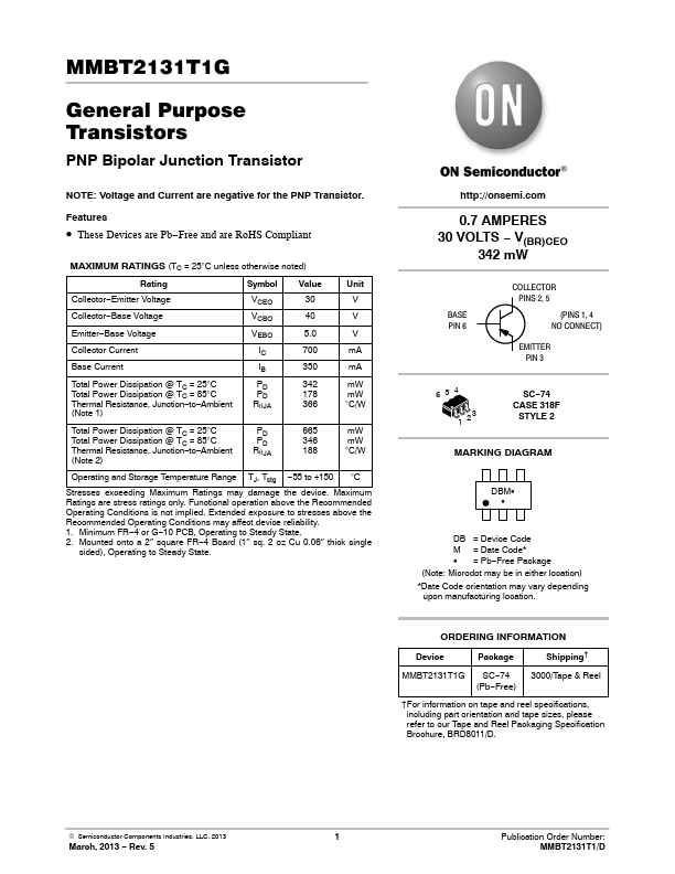
http://onsemi.com
0.7 AMPERES 30 VOLTS − V(BR)CEO
342 mW
BASE PIN 6
COLLECTOR PINS 2, 5
(PINS 1, 4 NO CONNECT)
EMITTER PIN 3
654 1 23
SC−74 CASE 318F
STYLE 2
MARKING DIAGRAM
DBMG G
DB = Device Code M = Date Code* G...