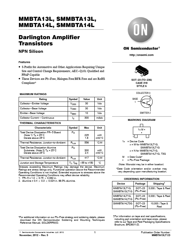
MMBTA13L, SMMBTA13L, MMBTA14L, SMMBTA14L
Darlington Amplifier Transistors
NPN Silicon
Features
• S Prefix for Automotiv...
MMBTA13L, SMMBTA13L, MMBTA14L, SMMBTA14L
Darlington Amplifier Transistors
NPN Silicon
Features
S Prefix for Automotive and Other Applications Requiring Unique
Site and Control Change Requirements; AEC−Q101 Qualified and PPAP Capable
These Devices are Pb−Free, Halogen Free/BFR Free and are RoHS
Compliant*
MAXIMUM RATINGS
Rating
Symbol Value
Unit
Collector −Emitter
Voltage Collector −Base
Voltage Emitter −Base
Voltage Collector Current − Continuous THERMAL CHARACTERISTICS
VCES VCBO VEBO
IC
30 Vdc 30 Vdc 10 Vdc 300 mAdc
Characteristic
Symbol
Max
Unit
Total Device Dissipation FR− 5 Board (Note 1) TA = 25°C Derate above 25°C
PD 225 mW 1.8 mW/°C
Thermal Resistance, Junction−to−Ambient Total Device Dissipation Alumina
Substrate, (Note 2) TA = 25°C Derate above 25°C
RqJA PD
556 °C/W 300 mW 2.4 mW/°C
Thermal Resistance, Junction−to−Ambient RqJA
417 °C/W
Junction and Storage Temperature
TJ, Tstg −55 to +150 °C
Stresses exceeding Maximum Ratings may damage the device. Maximum Ratings are stress ratings only. Functional operation above the Recommended Operating Conditions is not implied. Extended exposure to stresses above the Recommended Operating Conditions may affect device reliability. 1. FR−5 = 1.0 0.75 0.062 in. 2. Alumina = 0.4 0.3 0.024 in. 99.5% alumina.
*For additional information on our Pb−Free strategy and soldering details, please download the ON Semiconductor Soldering and Mounting Techniques Reference Manual, SOLDERRM/D.
© Semiconductor ...