MN101CF70C
www.DataSheet4U.com
MN101C70C
MN101C70C Mask ROM 48K 2K LQFP080-P-1414A, TQFP080-P-1212D (Under planning) 0.1 µs (at 3....
Description
www.DataSheet4U.com
MN101C70C
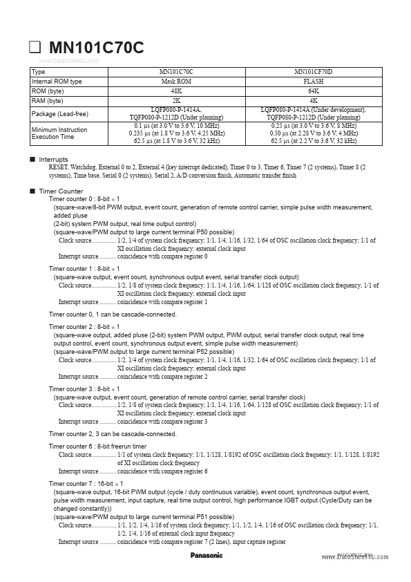
MN101C70C Mask ROM 48K 2K LQFP080-P-1414A, TQFP080-P-1212D (Under planning) 0.1 µs (at 3.0 V to 3.6 V, 10 MHz) 0.235 µs (at 1.8 V to 3.6 V, 4.25 MHz) 62.5 µs (at 1.8 V to 3.6 V, 32 kHz) MN101CF70D FLASH 64K 4K LQFP080-P-1414A (Under development), TQFP080-P-1212D (Under planning) 0.25 µs (at 3.0 V to 3.6 V, 8 MHz) 0.50 µs (at 2.28 V to 3.6 V, 4 MHz) 62.5 µs (at 2.2 V to 3.6 V, 32 kHz)
Type Internal ROM type ROM (byte) RAM (byte) Package (Lead-free) Minimum Instruction Execution Time
Interrupts
RESET, Watchdog, External 0 to 2, External 4 (key interrupt dedicated), Timer 0 to 3, Timer 6, Timer 7 (2 systems), Timer 8 (2 systems), Time base, Serial 0 (2 systems), Serial 2, A/D conversion finish, Automatic transfer finish Timer counter 0 : 8-bit × 1 (square-wave/8-bit PWM output, event count, generation of remote control carrier, simple pulse width measurement, added pluse (2-bit) system PWM output, real time output control) (square-wave/PWM output to large current terminal P50 possible) Clock source................ 1/2, 1/4 of system clock frequency; 1/1, 1/4, 1/16, 1/32, 1/64 of OSC oscillation clock frequency; 1/1 of XI oscillation clock frequency; external clock input Interrupt source ........... coincidence with compare register 0 Timer counter 1 : 8-bit × 1 (square-wave output, event count, synchronous output event, serial transfer clock output) Clock source................ 1/2, 1/8 of system clock frequency; 1/1, 1/4, 1/16, 1/64, 1/128 of O...
Similar Datasheet