MOTOROLA
SEMICONDUCTOR TECHNICAL DATA
Order this document by MPS6601/D
Amplifier Transistors
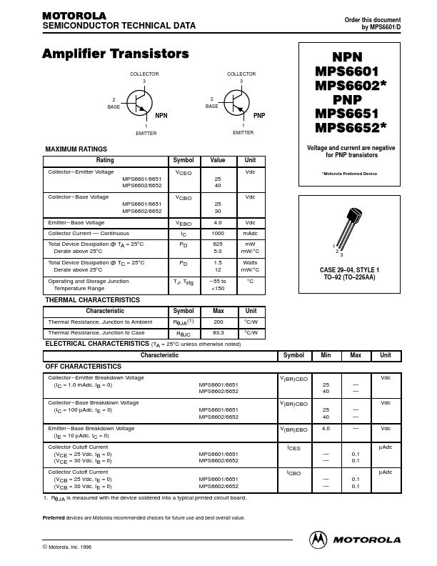
COLLECTOR 3 2 BASE NPN 1...
MOTOROLA
SEMICONDUCTOR TECHNICAL DATA
Order this document by MPS6601/D
Amplifier Transistors
COLLECTOR 3 2 BASE NPN 1 EMITTER 2 BASE PNP 1 EMITTER COLLECTOR 3
NPN MPS6601 MPS6602* PNP MPS6651 MPS6652*
Voltage and current are negative for PNP transistors
*Motorola Preferred Device
MAXIMUM RATINGS
Rating Collector – Emitter
Voltage MPS6601/6651 MPS6602/6652 Collector – Base
Voltage MPS6601/6651 MPS6602/6652 Emitter – Base
Voltage Collector Current — Continuous Total Device Dissipation @ TA = 25°C Derate above 25°C Total Device Dissipation @ TC = 25°C Derate above 25°C Operating and Storage Junction Temperature Range VEBO IC PD PD TJ, Tstg VCBO 25 30 4.0 1000 625 5.0 1.5 12 – 55 to +150 Vdc mAdc mW mW/°C Watts mW/°C °C Symbol VCEO 25 40 Vdc Value Unit Vdc
1 2 3
CASE 29–04, STYLE 1 TO–92 (TO–226AA)
THERMAL CHARACTERISTICS
Characteristic Thermal Resistance, Junction to Ambient Thermal Resistance, Junction to Case Symbol RqJA(1) RqJC Max 200 83.3 Unit °C/W °C/W
ELECTRICAL CHARACTERISTICS (TA = 25°C unless otherwise noted)
Characteristic Symbol Min Max Unit
OFF CHARACTERISTICS
Collector – Emitter Breakdown
Voltage (IC = 1.0 mAdc, IB = 0) Collector – Base Breakdown
Voltage (IC = 100 µAdc, IE = 0) Emitter – Base Breakdown
Voltage (IE = 10 µAdc, IC = 0) Collector Cutoff Current (VCE = 25 Vdc, IB = 0) (VCE = 30 Vdc, IB = 0) Collector Cutoff Current (VCB = 25 Vdc, IE = 0) (VCB = 30 Vdc, IE = 0) MPS6601/6651 MPS6602/6652 ICBO MPS6601/6651 MPS6602/6652 — — 0.1 0.1 V(BR)CEO MPS660...