MOTOROLA
SEMICONDUCTOR TECHNICAL DATA
Order this document by MPS6714/D
One Watt Amplifier Transistors
NPN Silicon
COL...
MOTOROLA
SEMICONDUCTOR TECHNICAL DATA
Order this document by MPS6714/D
One Watt Amplifier Transistors
NPN Silicon
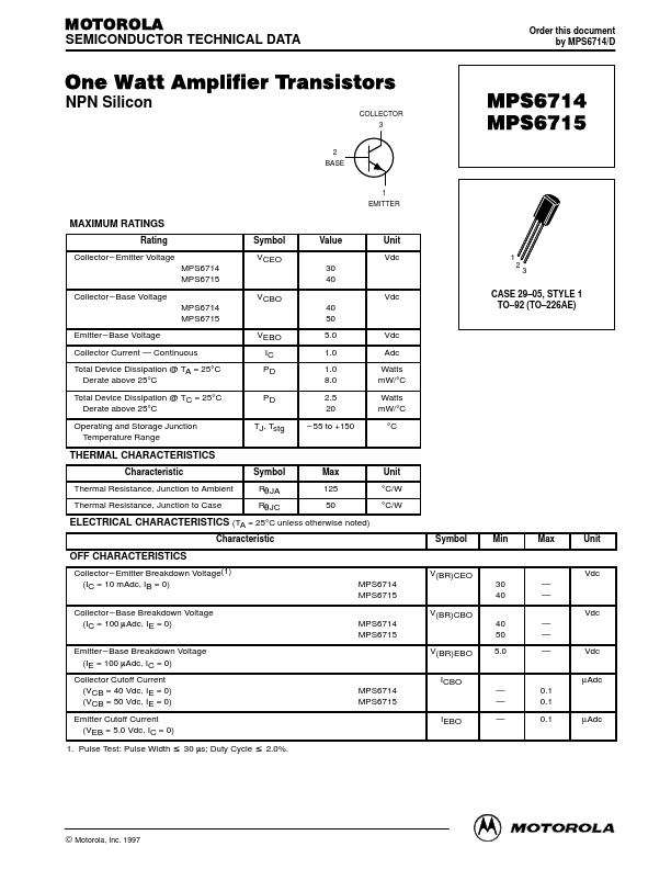
COLLECTOR 3 2 BASE 1 EMITTER
MPS6714 MPS6715
MAXIMUM RATINGS
Rating Collector – Emitter
Voltage MPS6714 MPS6715 Collector – Base
Voltage MPS6714 MPS6715 Emitter – Base
Voltage Collector Current — Continuous Total Device Dissipation @ TA = 25°C Derate above 25°C Total Device Dissipation @ TC = 25°C Derate above 25°C Operating and Storage Junction Temperature Range VEBO IC PD PD TJ, Tstg VCBO 40 50 5.0 1.0 1.0 8.0 2.5 20 – 55 to +150 Vdc Adc Watts mW/°C Watts mW/°C °C Symbol VCEO 30 40 Vdc Value Unit Vdc
1 2 3
CASE 29–05, STYLE 1 TO–92 (TO–226AE)
THERMAL CHARACTERISTICS
Characteristic Thermal Resistance, Junction to Ambient Thermal Resistance, Junction to Case Symbol RqJA RqJC Max 125 50 Unit °C/W °C/W
ELECTRICAL CHARACTERISTICS (TA = 25°C unless otherwise noted)
Characteristic Symbol Min Max Unit
OFF CHARACTERISTICS
Collector – Emitter Breakdown
Voltage(1) (IC = 10 mAdc, IB = 0) Collector – Base Breakdown
Voltage (IC = 100 mAdc, IE = 0) Emitter – Base Breakdown
Voltage (IE = 100 mAdc, IC = 0) Collector Cutoff Current (VCB = 40 Vdc, IE = 0) (VCB = 50 Vdc, IE = 0) Emitter Cutoff Current (VEB = 5.0 Vdc, IC = 0) 1. Pulse Test: Pulse Width MPS6714 MPS6715 IEBO V(BR)CEO MPS6714 MPS6715 V(BR)CBO MPS6714 MPS6715 V(BR)EBO ICBO — — — 0.1 0.1 0.1 µAdc 40 50 5.0 — — — Vdc µAdc 30 40 — — Vdc Vdc
v 30 ms; Duty Cycle v 2.0%.
Motorola Small–Signal Transistors, FETs and ...